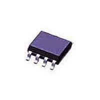
TISPPBL1DR Bourns Inc., TISPPBL1DR Datasheet - Page 9

TISPPBL1DR
Manufacturer Part Number
TISPPBL1DR
Description
Sidacs SURGE SUP 8-SOP
Manufacturer
Bourns Inc.
Datasheet
1.TISPPBL3SE.pdf
(18 pages)
Specifications of TISPPBL1DR
Mounting Style
SMD/SMT
Package / Case
SO-8
Lead Free Status / RoHS Status
Lead free / RoHS Compliant
Available stocks
Company
Part Number
Manufacturer
Quantity
Price
Company:
Part Number:
TISPPBL1DR
Manufacturer:
STM
Quantity:
21 600
Part Number:
TISPPBL1DR
Manufacturer:
TI/德州仪器
Quantity:
20 000
TISPPBLx limiting voltages
test circuit
impulse generator
AUGUST 1997 - REVISED AUGUST 2002
Specifications are subject to change without notice.
Figure 13 NEGATIVE OVERVOLTAGE CONDITION
P R O D U C T
conducted by the principal terminals. The gate current is positive during clipping (charging the V
negative when the thyristor is on or the diode is conducting (loading the V
current and the reduced level of positive gate current the V
100 mA. As the V
result, the SLIC could be destroyed by the voltage of V
capability on the V
Fast rising impulses will cause short term overshoots in gate-cathode voltage. The negative protection
voltage under impulse conditions will also be increased if there is a long connection between the gate
decoupling capacitor, C1, and the gate terminal. During the initial rise of a fast impulse, the gate current (I
the same as the cathode current (I
printed wiring track. To minimise this inductive voltage increase of protection voltage, the length of the
capacitor to gate terminal tracking should be minimised. Inductive voltages in the protector cathode wiring
can increase the protection voltage. These voltages can be minimised by routing the SLIC connection through
the protector as shown in Figure 13 and Figure 14.
Positive overvoltages (Figure 14) are clipped to ground by forward conduction of the diode section in the
TISPPBLx. Fast rising impulses will cause short term overshoots in forward voltage (V
This clause details the TISPPBLx voltage limiting levels under impulse conditions.
Figure 3 shows the basic test circuit used for the measurement of impulse limiting voltage. During the
impulse, the high levels of electrical energy and rapid rates of change cause electrical noise to be induced or
conducted into the measurement system. It is possible for the electrical noise voltage to be many times the
wanted signal voltage. Elaborate wiring and measurement techniques where used to reduce the noise
voltage to less than 2 V peak to peak.
A Keytek ECAT E-Class series 100 with an E502 surge network was used for testing. The E502 produces a
0.5/700 voltage impulse. This particular waveform was used as it has the fastest rate of current rise (di/dt) of
the commonly used lightning surge waveforms. This maximises the measured limiting voltage. Figure 4
shows the current wavefront through the DUT. To produce a peak test current level of ±20 A, the E502
charging voltage was set to ±1960 V. Figure 5 shows the DUT current di/dt. Initially the wavefront current rises
AI6XANB
PROTECTION
TISPPBLx
I
T
V
SLIC
B
I N F O R M A T I O N
B
BAT
supply is likely to be electronic it would not be designed to be charged like a battery. As a
Th4
Th5
C1
pin. The integrated transistor buffer removes this problem.
D1
V
SLIC
Bat
C2
K
). Rates of 60 A/µs can cause inductive voltages of 0.6 V in 2.5 cm of
DUAL FORWARD-CONDUCTING P-GATE THYRISTORS
TISPPBL1D, TISPPBL1P, TISPPBL2D, TISPPBL2P
Figure 14 POSITIVE OVERVOLTAGE CONDITION
B
B
supply could be charged with a current of nearly
increasing to a level that exceeded the SLIC’s
FOR ERICSSON COMPONENTS SLICS
AI6XAOB
I
F
PROTECTION
B
TISPPBLx
supply). Without the negative gate
V
SLIC
B
Th4
Th5
C1
FRM
D1
).
V
SLIC
Bat
C2
B
supply) and
G
) is
9


