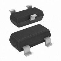
BAW56,215 NXP Semiconductors, BAW56,215 Datasheet - Page 10

BAW56,215
Manufacturer Part Number
BAW56,215
Description
DIODE SW DBL 90V 215MA HS SOT23
Manufacturer
NXP Semiconductors
Datasheet
1.BAW56235.pdf
(15 pages)
Specifications of BAW56,215
Package / Case
SOT-23-3, TO-236-3, Micro3™, SSD3, SST3
Voltage - Forward (vf) (max) @ If
1V @ 50mA
Current - Reverse Leakage @ Vr
500nA @ 80V
Current - Average Rectified (io) (per Diode)
215mA (DC)
Voltage - Dc Reverse (vr) (max)
90V
Reverse Recovery Time (trr)
4ns
Diode Type
Standard
Speed
Fast Recovery =< 500ns, > 200mA (Io)
Diode Configuration
1 Pair Common Anode
Mounting Type
Surface Mount
Product
Switching Diodes
Peak Reverse Voltage
90 V
Forward Continuous Current
0.215 A
Max Surge Current
4 A
Configuration
Dual Common Anode
Recovery Time
4 ns
Forward Voltage Drop
1.25 V
Maximum Reverse Leakage Current
0.5 uA
Operating Temperature Range
+ 150 C
Maximum Operating Temperature
+ 150 C
Minimum Operating Temperature
- 65 C
Mounting Style
SMD/SMT
Rectifier Type
Switching Diode
Peak Rep Rev Volt
90V
Avg. Forward Curr (max)
0.215A
Rev Curr
0.5uA
Peak Non-repetitive Surge Current (max)
4A
Forward Voltage
1.25V
Operating Temp Range
-65C to 150C
Package Type
TO-236AB
Rev Recov Time
4ns
Operating Temperature Classification
Military
Mounting
Surface Mount
Pin Count
3
Lead Free Status / RoHS Status
Lead free / RoHS Compliant
Lead Free Status / RoHS Status
Lead free / RoHS Compliant, Lead free / RoHS Compliant
Other names
568-1626-2
933098990215
BAW56 T/R
933098990215
BAW56 T/R
Available stocks
Company
Part Number
Manufacturer
Quantity
Price
Part Number:
BAW56,215
Manufacturer:
NEXPERIA/安世
Quantity:
20 000
NXP Semiconductors
BAV756S_BAW56_SER_5
Product data sheet
Fig 13. Wave soldering footprint BAW56 (SOT23/TO-236AB)
Fig 14. Reflow soldering footprint BAW56M (SOT883/SC-101)
4.60
Reflow soldering is the only recommended soldering method.
4.00
1.20
0.90
R = 0.05 (12 )
0.20
Rev. 05 — 26 November 2007
0.35
0.25
(2 )
(2 )
solder lands
solder paste
2
3.40
2.80
4.50
0.30
0.40
0.50
(2 )
(2 )
(2 )
3
1.20 (2x)
BAV756S; BAW56 series
1
1.30
0.30
solder resist
occupied area
Dimensions in mm
preferred transport direction during soldering
0.30
0.40
0.50
Dimensions in mm
High-speed switching diodes
solder lands
solder resist
occupied area
R = 0.05 (12 )
0.60 0.70 0.80
© NXP B.V. 2007. All rights reserved.
sot023
10 of 15


