BYV32-200G ON Semiconductor, BYV32-200G Datasheet
BYV32-200G
Specifications of BYV32-200G
Available stocks


Related parts for BYV32-200G


BYV32-200G Summary of contents
Page 1
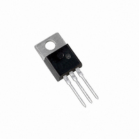
... Assembly Location Y = Year WW = Work Week BYV32−200 = Device Code G = Pb−Free Package AKA = Diode Polarity ORDERING INFORMATION Device Package BYV32−200 TO−220 BYV32−200G TO−220 (Pb−Free MARKING DIAGRAM AYWW BYV32-200G AKA Shipping 50 Units / Rail 50 Units / Rail Publication Order Number: BYV32−200/D ...
Page 2
MAXIMUM RATINGS Peak Repetitive Reverse Voltage Working Peak Reverse Voltage DC Blocking Voltage Average Rectified Forward Current 156°C C Per Leg Total Device Peak Rectified Forward Current (Square Wave, 20 kHz 154°C − Per Diode Leg ...
Page 3
T = 175° 7.0 5.0 3.0 2.0 1.0 0.7 0.5 0.3 0.2 0.1 0.2 0.3 0.4 0.5 0.6 0.7 0.8 v INSTANTANEOUS VOLTAGE (VOLTS) F, Figure 1. Typical Forward Voltage, Per Leg 20 ...
Page 4
Duty Cycle 20 0.1 Single Pulse 0.01 0.001 0.000001 0.00001 0.0001 Figure ...
Page 5
... S 0.045 0.055 1.15 1.39 T 0.235 0.255 5.97 6.47 U 0.000 0.050 0.00 1.27 V 0.045 --- 1.15 --- Z --- 0.080 --- 2.04 STYLE 6: PIN 1. ANODE 2. CATHODE 3. ANODE 4. CATHODE ON Semiconductor Website: www.onsemi.com Order Literature: http://www.onsemi.com/orderlit For additional information, please contact your local Sales Representative BYV32−200/D ...