MBR140SFT1G ON Semiconductor, MBR140SFT1G Datasheet - Page 2
MBR140SFT1G
Manufacturer Part Number
MBR140SFT1G
Description
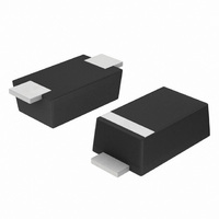
DIODE SCHOTTKY 40V 1A SOD123FL
Manufacturer
ON Semiconductor
Datasheet
1.MBR140SFT1G.pdf
(6 pages)
Specifications of MBR140SFT1G
Voltage - Forward (vf) (max) @ If
550mV @ 1A
Voltage - Dc Reverse (vr) (max)
40V
Current - Average Rectified (io)
1A
Current - Reverse Leakage @ Vr
500µA @ 40V
Diode Type
Schottky
Speed
Fast Recovery =< 500ns, > 200mA (Io)
Mounting Type
Surface Mount
Package / Case
SOD-123 Flat Leads
Product
Schottky Diodes
Peak Reverse Voltage
40 V
Forward Continuous Current
1 A
Max Surge Current
30 A
Configuration
Single
Forward Voltage Drop
0.85 V @ 3 A
Maximum Reverse Leakage Current
500 uA
Operating Temperature Range
- 55 C to + 125 C
Mounting Style
SMD/SMT
Dc
09+
Lead Free Status / RoHS Status
Lead free / RoHS Compliant
Reverse Recovery Time (trr)
-
Capacitance @ Vr, F
-
Lead Free Status / Rohs Status
Lead free / RoHS Compliant
Other names
MBR140SFT1GOSTR
Available stocks
Company
Part Number
Manufacturer
Quantity
Price
Company:

Part Number:
MBR140SFT1G
Manufacturer:
ON
Quantity:
30 000
Company:
Part Number:
MBR140SFT1G
Manufacturer:
ON
Quantity:
11 000
Company:
Part Number:
MBR140SFT1G
Manufacturer:
ON
Quantity:
30 000
Part Number:
MBR140SFT1G
Manufacturer:
ON/安森美
Quantity:
20 000


Maximum ratings are those values beyond which device damage can occur. Maximum ratings applied to the device are individual stress limit
values (not normal operating conditions) and are not valid simultaneously. If these limits are exceeded, device functional operation is not implied,
damage may occur and reliability may be affected.
1. Mounted with minimum recommended pad size, PC Board FR4.
2. Mounted with 1 in. copper pad (Cu area 700 mm
3. Pulse Test: Pulse Width ≤ 250 ms, Duty Cycle ≤ 2%.
MAXIMUM RATINGS
THERMAL CHARACTERISTICS
ELECTRICAL CHARACTERISTICS
Peak Repetitive Reverse Voltage
Average Rectified Forward Current (At Rated V
Peak Repetitive Forward Current
Non−Repetitive Peak Surge Current
Storage Temperature
Operating Junction Temperature
Voltage Rate of Change (Rated V
Thermal Resistance, Junction−to−Lead (Note 1)
Thermal Resistance, Junction−to−Lead (Note 2)
Thermal Resistance, Junction−to−Ambient (Note 1)
Thermal Resistance, Junction−to−Ambient (Note 2)
Maximum Instantaneous Forward Voltage (Note 3), See Figure 2
Maximum Instantaneous Reverse Current (Note 3), See Figure 4
(I
(I
(I
(V
(V
Working Peak Reverse Voltage
DC Blocking Voltage
(At Rated V
(Non−Repetitive peak surge current, halfwave, single phase, 60 Hz)
F
F
F
R
R
= 0.1 A)
= 1.0 A)
= 3.0 A)
= 40 V)
= 20 V)
R
, Square Wave, 100 kHz, T
R
, T
Rating
J
= 25°C)
L
= 95°C)
R
, T
2
).
L
= 112°C)
http://onsemi.com
MBR140SFT1
2
Symbol
V
V
dv/dt
I
I
T
R
R
FRM
FSM
RWM
V
R
R
RRM
V
I
T
I
stg
O
R
tja
tja
R
J
tjl
tjl
F
T
T
J
J
0.36
0.55
0.85
0.15
= 25°C
= 25°C
0.5
−55 to 150
−55 to 125
10,000
Value
325
1.0
2.0
40
30
26
21
82
T
T
J
J
0.515
0.30
0.88
= 85°C
= 85°C
25
18
°C/W
Unit
V/ms
mA
°C
°C
V
A
A
A
V
Related parts for MBR140SFT1G
Image
Part Number
Description
Manufacturer
Datasheet
Request
R

Part Number:
Description:
RELAY TIME ANALG 10A 24-240V DIN
Manufacturer:
Crouzet USA
Datasheet:

Part Number:
Description:
ON Semiconductor [VOLTAGE REGULATOR]
Manufacturer:
ON Semiconductor
Datasheet:
Part Number:
Description:
357-036-542-201 CARDEDGE 36POS DL .156 BLK LOPRO
Manufacturer:
ON Semiconductor
Datasheet:
Part Number:
Description:
357-036-542-201 CARDEDGE 36POS DL .156 BLK LOPRO
Manufacturer:
ON Semiconductor
Datasheet:
Part Number:
Description:
357-036-542-201 CARDEDGE 36POS DL .156 BLK LOPRO
Manufacturer:
ON Semiconductor
Datasheet:
Part Number:
Description:
357-036-542-201 CARDEDGE 36POS DL .156 BLK LOPRO
Manufacturer:
ON Semiconductor
Datasheet:
Part Number:
Description:
357-036-542-201 CARDEDGE 36POS DL .156 BLK LOPRO
Manufacturer:
ON Semiconductor
Datasheet:
Part Number:
Description:
357-036-542-201 CARDEDGE 36POS DL .156 BLK LOPRO
Manufacturer:
ON Semiconductor
Datasheet:
Part Number:
Description:
357-036-542-201 CARDEDGE 36POS DL .156 BLK LOPRO
Manufacturer:
ON Semiconductor
Datasheet:
Part Number:
Description:
357-036-542-201 CARDEDGE 36POS DL .156 BLK LOPRO
Manufacturer:
ON Semiconductor
Datasheet:
Part Number:
Description:
357-036-542-201 CARDEDGE 36POS DL .156 BLK LOPRO
Manufacturer:
ON Semiconductor
Datasheet:
Part Number:
Description:
357-036-542-201 CARDEDGE 36POS DL .156 BLK LOPRO
Manufacturer:
ON Semiconductor
Datasheet:
Part Number:
Description:
Manufacturer:
ON Semiconductor
Datasheet:
Part Number:
Description:
Manufacturer:
ON Semiconductor
Datasheet: