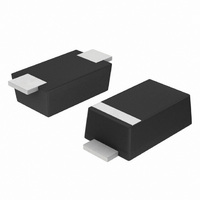
MBR140SFT1G ON Semiconductor, MBR140SFT1G Datasheet - Page 4

MBR140SFT1G
Manufacturer Part Number
MBR140SFT1G
Description
DIODE SCHOTTKY 40V 1A SOD123FL
Manufacturer
ON Semiconductor
Datasheet
1.MBR140SFT1G.pdf
(6 pages)
Specifications of MBR140SFT1G
Voltage - Forward (vf) (max) @ If
550mV @ 1A
Voltage - Dc Reverse (vr) (max)
40V
Current - Average Rectified (io)
1A
Current - Reverse Leakage @ Vr
500µA @ 40V
Diode Type
Schottky
Speed
Fast Recovery =< 500ns, > 200mA (Io)
Mounting Type
Surface Mount
Package / Case
SOD-123 Flat Leads
Product
Schottky Diodes
Peak Reverse Voltage
40 V
Forward Continuous Current
1 A
Max Surge Current
30 A
Configuration
Single
Forward Voltage Drop
0.85 V @ 3 A
Maximum Reverse Leakage Current
500 uA
Operating Temperature Range
- 55 C to + 125 C
Mounting Style
SMD/SMT
Dc
09+
Lead Free Status / RoHS Status
Lead free / RoHS Compliant
Reverse Recovery Time (trr)
-
Capacitance @ Vr, F
-
Lead Free Status / Rohs Status
Lead free / RoHS Compliant
Other names
MBR140SFT1GOSTR
Available stocks
Company
Part Number
Manufacturer
Quantity
Price
Company:
Part Number:
MBR140SFT1G
Manufacturer:
ON
Quantity:
30 000
Company:
Part Number:
MBR140SFT1G
Manufacturer:
ON
Quantity:
11 000
Company:
Part Number:
MBR140SFT1G
Manufacturer:
ON
Quantity:
30 000
Part Number:
MBR140SFT1G
Manufacturer:
ON/安森美
Quantity:
20 000
1000
1000
100
100
10
0.1
10
* Reverse power dissipation and the possibility of thermal runaway must be considered when operating this device under any re-
verse voltage conditions. Calculations of T
T
This graph displays the derated allowable T
where r(t) = Rthja. For other power applications further calculations must be performed.
1
J
0
0.000001
may be calculated from the equation:
5
V
0.00001
R
10
, REVERSE VOLTAGE (VOLTS)
Figure 7. Capacitance
0.05
0.01
D = 0.5
0.2
0.1
15
SINGLE PULSE
0.0001
20
25
T
J
0.001
J
J
= 25°C
therefore must include forward and reverse power effects. The allowable operating
due to reverse bias under DC conditions only and is calculated as T
30
Figure 9. Thermal Response
T
r(t) = thermal impedance under given conditions,
Pf = forward power dissipation, and
Pr = reverse power dissipation
J
Test Type > Min Pad < Die Size 38x38 @ 75% mils
= T
35
http://onsemi.com
Jmax
MBR140SFT1
t
1
− r(t)(Pf + Pr) where
0.01
, TIME (sec)
40
4
125
105
115
95
85
75
65
55
0
0.1
324.9°C/W
Figure 8. Typical Operating Temperature
5
V
R
, DC REVERSE VOLTAGE (VOLTS)
10
1
235°C/W
15
130°C/W
Derating*
20
10
R
qJA
P
DUTY CYCLE, D = t
(pk)
25
qJA = 321.8 °C/W
= 25.6°C/W
J
= T
Jmax
100
30
t
1
t
2
− r(t)Pr,
35
1
/t
2
1000
40


