STGW35NC60WD STMicroelectronics, STGW35NC60WD Datasheet
STGW35NC60WD
Specifications of STGW35NC60WD
STGW35NC60WD
Available stocks


Related parts for STGW35NC60WD


STGW35NC60WD Summary of contents
Page 1
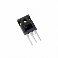
... Table 1. Device summary Order code STGW35NC60WD November 2008 40 A, 600 V ultra fast IGBT Figure 1. Marking Package GW35NC60WD TO-247 long leads Rev 2 STGW35NC60WD TO-247 long leads Internal schematic diagram Packaging Tube www.st.com 1/14 14 ...
Page 2
... Contents Contents 1 Electrical ratings . . . . . . . . . . . . . . . . . . . . . . . . . . . . . . . . . . . . . . . . . . . . 3 2 Electrical characteristics . . . . . . . . . . . . . . . . . . . . . . . . . . . . . . . . . . . . . 4 2.1 Electrical characteristics (curves) 3 Test circuit . . . . . . . . . . . . . . . . . . . . . . . . . . . . . . . . . . . . . . . . . . . . . . . 10 4 Package mechanical data . . . . . . . . . . . . . . . . . . . . . . . . . . . . . . . . . . . . 11 5 Revision history . . . . . . . . . . . . . . . . . . . . . . . . . . . . . . . . . . . . . . . . . . . 13 2/14 STGW35NC60WD . . . . . . . . . . . . . . . . . . . . . . . . . . . . . 7 ...
Page 3
... STGW35NC60WD 1 Electrical ratings Table 2. Absolute maximum ratings Symbol V Collector-emitter voltage (V CES (1) Collector current (continuous ° (1) Collector current (continuous) at 100 ° (2) Collector current (pulsed (3) Turn-off latching current Gate-emitter voltage GE I Diode RMS forward current Surge not repetitive forward current t FSM P Total dissipation at T ...
Page 4
... Parameter Test conditions 600 600 ± Parameter Test conditions MHz 390 (see Figure 18) STGW35NC60WD Min. Typ. Max. Unit 600 = A,T = 125 °C 1 250 µA 3. 125 ° Min. Typ. Max. Unit 2080 175 102 5.75 V 250 µ ± 100 140 nC ...
Page 5
... STGW35NC60WD Table 6. Switching on/off (inductive load) Symbol t Turn-on delay time d(on) t Current rise time r Turn-on current slope (di/dt Turn-on delay time d(on) t Current rise time r Turn-on current slope (di/dt Off voltage rise time r off Turn-off delay time d off Current fall time ...
Page 6
... Reverse recovery current I rrm t Reverse recovery time rr Q Reverse recovery charge rr Reverse recovery current I rrm 6/14 Parameter Test conditions A di/dt = 100 A/µs (see Figure 20 A =125 °C, di/dt = 100 A/µs C (see Figure 20) STGW35NC60WD Min. Typ. Max. 2.6 = 125 ° 180 4.5 Unit ...
Page 7
... STGW35NC60WD 2.1 Electrical characteristics (curves) Figure 2. Output characteristics Figure 4. Transconductance Figure 6. Gate charge vs gate-source voltage Figure 7. Electrical characteristics Figure 3. Transfer characteristics Figure 5. Collector-emitter on voltage vs temperature V ( 40A 30A 3 2.8 20A 2.6 2.4 2.2 2 1.8 I =10A C 1.6 1.4 -75 -50 - Capacitance variations ...
Page 8
... Figure 10. Normalized breakdown voltage vs temperature Figure 12. Switching losses vs gate resistance Figure 13. Switching losses vs collector 8/14 Figure 9. Collector-emitter on voltage vs collector current V CE(sat) (V) 3.2 T =-50° =25°C 2.8 J 2.6 2.4 2.2 2 1.8 1.6 1.4 1 Figure 11. Switching losses vs temperature current STGW35NC60WD HV28950 T =150° (A) C ...
Page 9
... STGW35NC60WD Figure 14. Thermal impedance Figure 16. Emitter-collector diode characteristics IFM(A) 120 110 Tj=125˚C Tj=125˚C (Maximum values) (Maximum values) 100 90 80 Tj=125˚C Tj=125˚C 70 (Typical values) (Typical values VFM( Figure 15. Turn-off SOA Tj=25˚C (Maximum values Electrical characteristics 9/14 ...
Page 10
... Test circuit Figure 17. Test circuit for inductive load switching Figure 19. Switching waveform Td(off) Td(on) Tr(Ion) Ton 10/14 Figure 18. Gate charge test circuit AM01504v1 Figure 20. Diode recovery time waveform 90% 10 90% 10% Tr(Voff) Tcross 90% 10% Tf Toff AM01506v1 STGW35NC60WD Q di/ RRM RRM V di/dt AM01505v1 AM01507v1 ...
Page 11
... STGW35NC60WD 4 Package mechanical data In order to meet environmental requirements, ST offers these devices in ECOPACK® packages. These packages have a Lead-free second level interconnect. The category of second level interconnect is marked on the package and on the inner box label, in compliance with JEDEC Standard JESD97. The maximum ratings related to soldering conditions are also marked on the inner box label ...
Page 12
... TO-247 long leads mechanical data mm Min. Typ. 4.85 2.2 0.4 1 1.9 3 10.9 15.45 19.85 3.7 18.3 14.2 34.05 5.35 2 60° 3.55 STGW35NC60WD Max. 5.16 2.6 0.8 1 2.4 3.4 16.03 21.09 4.3 19.13 20.3 41.38 6.3 3 5° 3.65 7395426_Rev_D ...
Page 13
... STGW35NC60WD 5 Revision history Table 9. Document revision history Date 12-Jul-2007 11-Nov-2008 Revision 1 Initial release. 2 Document status promoted from preliminary data to datasheet. Revision history Changes 13/14 ...
Page 14
... Australia - Belgium - Brazil - Canada - China - Czech Republic - Finland - France - Germany - Hong Kong - India - Israel - Italy - Japan - Malaysia - Malta - Morocco - Singapore - Spain - Sweden - Switzerland - United Kingdom - United States of America 14/14 Please Read Carefully: © 2008 STMicroelectronics - All rights reserved STMicroelectronics group of companies www.st.com STGW35NC60WD ...