IRG4PH40UDPBF International Rectifier, IRG4PH40UDPBF Datasheet - Page 2
IRG4PH40UDPBF
Manufacturer Part Number
IRG4PH40UDPBF
Description
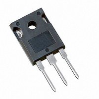
IGBT W/DIODE 1200V 30A TO247AC
Manufacturer
International Rectifier
Type
Ultrafastr
Datasheets
1.IRG4PH40UDPBF.pdf
(11 pages)
2.IRG4PH40UDPBF.pdf
(3 pages)
3.IRG4PH40UDPBF.pdf
(11 pages)
Specifications of IRG4PH40UDPBF
Voltage - Collector Emitter Breakdown (max)
1200V
Vce(on) (max) @ Vge, Ic
3.1V @ 15V, 21A
Current - Collector (ic) (max)
41A
Power - Max
160W
Input Type
Standard
Mounting Type
Through Hole
Package / Case
TO-247-3 (Straight Leads), TO-247AC
Channel Type
N
Configuration
Single
Collector-emitter Voltage
1.2kV
Gate To Emitter Voltage (max)
±20V
Package Type
TO-247AC
Pin Count
3 +Tab
Mounting
Through Hole
Operating Temperature (min)
-55
Operating Temperature (max)
150C
Operating Temperature Classification
Military
Capacitance, Gate
1800 pF
Current, Collector
41 A
Energy Rating
3.73 mJ
Polarity
N-Channel
Power Dissipation
160 W
Resistance, Thermal, Junction To Case
0.77 °C/W
Speed, Switching
40 kHz (Hard Switching), >200 kHz (Resonant Mode)
Voltage, Collector To Emitter Shorted
1200 V
Voltage, Collector To Emitter, Saturation
2.97 V
Transistor Type
IGBT
Dc Collector Current
41A
Collector Emitter Voltage Vces
1.2kV
Power Dissipation Pd
160W
Collector Emitter Voltage V(br)ceo
1.2kV
Operating Temperature Range
-55°C To +150°C
Rohs Compliant
Yes
Lead Free Status / RoHS Status
Lead free / RoHS Compliant
Igbt Type
-
Lead Free Status / Rohs Status
Compliant
Other names
*IRG4PH40UDPBF
Available stocks
Company
Part Number
Manufacturer
Quantity
Price
Company:

Part Number:
IRG4PH40UDPBF
Manufacturer:
NXP
Quantity:
3 000


IRG4PH40UDPbF
Switching Characteristics @ T
Electrical Characteristics @ T
Q
Qge
Q
t
t
t
t
E
E
E
t
t
t
t
E
L
C
C
C
t
I
Q
di
V
∆V
V
V
∆V
g
I
V
I
d(on)
r
d(off)
f
d(on)
r
d(off)
f
rr
rr
CES
GES
E
on
off
ts
ts
fe
ies
oes
res
(BR)CES
CE(on)
GE(th)
FM
g
gc
rr
(rec)M
(BR)CES
GE(th)
2
/dt
/∆T
/∆T
J
J
Total Gate Charge (turn-on)
Gate - Emitter Charge (turn-on)
Gate - Collector Charge (turn-on)
Turn-On Delay Time
Rise Time
Turn-Off Delay Time
Fall Time
Turn-On Switching Loss
Turn-Off Switching Loss
Total Switching Loss
Turn-On Delay Time
Rise Time
Turn-Off Delay Time
Fall Time
Total Switching Loss
Internal Emitter Inductance
Input Capacitance
Output Capacitance
Reverse Transfer Capacitance
Diode Reverse Recovery Time
Diode Peak Reverse Recovery Current
Diode Reverse Recovery Charge
Diode Peak Rate of Fall of Recovery
During t
Collector-to-Emitter Breakdown VoltageS
Temperature Coeff. of Breakdown Voltage
Collector-to-Emitter Saturation Voltage
Gate Threshold Voltage
Temperature Coeff. of Threshold Voltage
Forward Transconductance T
Zero Gate Voltage Collector Current
Diode Forward Voltage Drop
Gate-to-Emitter Leakage Current
Parameter
Parameter
b
J
J
= 25°C (unless otherwise specified)
= 25°C (unless otherwise specified)
1200
Min. Typ. Max. Units
Min. Typ. Max. Units
3.0
—
—
—
—
—
—
—
—
—
—
—
—
—
—
—
—
—
—
—
—
—
—
—
—
—
—
—
16
—
—
—
—
—
—
—
—
—
—
1800
1.80
1.93
3.73
7.04
0.43
2.43
2.97
2.47
240
240
510
120
106
140
335
133
4.5
6.2
-11
2.6
2.4
86
13
29
46
35
97
42
32
13
18
63
85
24
—
—
—
—
—
5000
±100
130
150
360
160
380
880
250
4.6
8.0
3.1
6.0
3.3
3.1
20
44
95
11
—
—
—
—
—
—
—
—
—
—
—
—
—
—
—
—
—
—
—
—
—
mV/°C V
V/°C
A/µs
mJ
mJ
µA
nA
nC
nH
nC
pF
ns
ns
ns
V
V
S
V
A
I
V
V
T
I
V
Energy losses include "tail" and
diode reverse recovery.
See Fig. 9, 10, 18
T
I
V
Energy losses include "tail" and
diode reverse recovery.
Measured 5mm from package
V
V
ƒ = 1.0MHz
T
T
T
T
T
T
T
T
V
V
I
I
I
V
V
V
V
I
I
V
C
C
C
C
C
C
C
C
J
J
J
J
J
J
J
J
J
J
CC
GE
GE
GE
GE
CC
GE
GE
CE
CE
CE
GE
GE
GE
= 21A
= 21A, V
= 21A, V
= 125°C
= 125°C
= 125°C
= 21A
= 41A
= 21A, T
= 8.0A
= 8.0A, T
= 25°C
= 150°C,
= 25°C
= 25°C
= 25°C
= 25°C
= 125°C
= 400V
= 15V
= 15V, R
= 15V, R
= 0V
= 30V
= 0V, I
= 0V, I
= V
= V
= 100V, I
= 0V, V
= 0V, V
= ±20V
GE
GE
, I
, I
CC
CC
J
C
C
J
CE
CE
See Fig.
See Fig.
C
C
Conditions
= 150°C
Conditions
See Fig.
See Fig.
= 250µA
= 1.0mA
= 125°C
G
G
C
= 800V
= 800V
= 250µA
= 250µA
See Fig. 11, 18
= 600V, T
= 10Ω
= 10Ω
= 600V
= 21A
15
14
17
16
See Fig. 8
See Fig. 7
www.irf.com
di/dt = 200A/µs
V
See Fig. 2, 5
See Fig. 13
V
J
GE
I
R
= 150°C
F
= 200V
= 8.0A
= 15V
Related parts for IRG4PH40UDPBF
Image
Part Number
Description
Manufacturer
Datasheet
Request
R

Part Number:
Description:
SCHOTTKY RECTIFIER
Manufacturer:
International Rectifier Corp.
Datasheet:
Part Number:
Description:
SCHOTTKY RECTIFIER
Manufacturer:
International Rectifier Corp.
Datasheet:
Part Number:
Description:
SCHOTTKY RECTIFIER
Manufacturer:
International Rectifier Corp.
Datasheet:
Part Number:
Description:
SCHOTTKY RECTIFIER
Manufacturer:
International Rectifier Corp.
Datasheet:
Part Number:
Description:
SCHOTTKY RECTIFIER
Manufacturer:
International Rectifier Corp.
Datasheet:
Part Number:
Description:
SCHOTTKY RECTIFIER
Manufacturer:
International Rectifier Corp.
Datasheet:
Part Number:
Description:
SCHOTTKY RECTIFIER
Manufacturer:
International Rectifier Corp.
Datasheet:
Part Number:
Description:
SCHOTTKY RECTIFIER
Manufacturer:
International Rectifier Corp.
Datasheet:
Part Number:
Description:
SCHOTTKY RECTIFIER
Manufacturer:
International Rectifier Corp.
Datasheet:
Part Number:
Description:
SCHOTTKY RECTIFIER
Manufacturer:
International Rectifier Corp.
Datasheet:
Part Number:
Description:
SCHOTTKY RECTIFIER
Manufacturer:
International Rectifier Corp.
Datasheet:
Part Number:
Description:
SCHOTTKY RECTIFIER
Manufacturer:
International Rectifier Corp.
Datasheet:
Part Number:
Description:
SCHOTTKY RECTIFIER
Manufacturer:
International Rectifier Corp.
Datasheet:
Part Number:
Description:
SCHOTTKY RECTIFIER
Manufacturer:
International Rectifier Corp.
Datasheet:
Part Number:
Description:
SCHOTTKY RECTIFIER
Manufacturer:
International Rectifier Corp.
Datasheet: