IRG4PSH71UDPBF International Rectifier, IRG4PSH71UDPBF Datasheet - Page 2
IRG4PSH71UDPBF
Manufacturer Part Number
IRG4PSH71UDPBF
Description
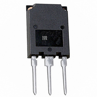
IGBT W/DIODE 1200V 99A SUPER247
Manufacturer
International Rectifier
Datasheet
1.IRG4PSH71UDPBF.pdf
(11 pages)
Specifications of IRG4PSH71UDPBF
Voltage - Collector Emitter Breakdown (max)
1200V
Vce(on) (max) @ Vge, Ic
2.7V @ 15V, 70A
Current - Collector (ic) (max)
99A
Power - Max
350W
Input Type
Standard
Mounting Type
Through Hole
Package / Case
Super-247-3 (Straight Leads)
Transistor Type
IGBT
Dc Collector Current
99A
Collector Emitter Voltage Vces
2.7V
Power Dissipation Pd
350W
Collector Emitter Voltage V(br)ceo
1.2kV
Operating Temperature Range
-5°C To +150°C
Rohs Compliant
Yes
Package
TO-274AA
Circuit
Co-Pack
Switching
Hard
Switching Speed
ULTRAFAST 8-30 kHz
Vces (v)
1200
Ic @ 25c (a)
99
Ic @ 100c (a)
50
Vce(on)@25c Typ (v)
2.52
Vce(on)@25c Max (v)
2.70
Ets Typ (mj)
18.2
Ets Max (mj)
19.7
Vf Typ
2.92
Pd @25c (w)
350
Environmental Options
PbF
Lead Free Status / RoHS Status
Lead free / RoHS Compliant
Igbt Type
-
Other names
*IRG4PSH71UDPBF
Available stocks
Company
Part Number
Manufacturer
Quantity
Price
Company:

Part Number:
IRG4PSH71UDPBF
Manufacturer:
IXYS
Quantity:
30 000


IRG4PSH71UDPbF
∆V
∆V
Electrical Characteristics @ T
V
V
V
V
gfe
I
V
I
Switching Characteristics @ T
Q
Q
Q
t
t
t
t
E
E
E
t
t
t
t
E
L
C
C
C
t
I
Q
di
CES
GES
d(on)
r
d(off)
f
d(on)
r
d(off)
f
rr
rr
E
(BR)CES
(BR)ECS
CE(on)
GE(th)
FM
on
off
tot
TS
ies
oes
res
g
ge
gc
rr
(rec)M
2
(BR)CES
GE(th)
/dt
/∆T
/∆T
J
J
Collector-to-Emitter Breakdown Voltage
Emitter-to-Collector Breakdown Voltage
Temperature Coeff. of Breakdown Voltage
Collector-to-Emitter Saturation Voltage
Gate Threshold Voltage
Threshold Voltage temp. coefficient
Zero Gate Voltage Collector Current
Diode Forward Voltage Drop
Gate-to-Emitter Leakage Current
Total Gate Charge (turn-on)
Gate-to-Emitter Charge (turn-on)
Gate-to-Collector Charge (turn-on)
Turn-On delay time
Rise time
Turn-Off delay time
Fall time
Turn-On Switching Loss
Turn-Off Switching Loss
Total Switching Loss
Turn-On delay time
Rise time
Turn-Off delay time
Fall time
Total Switching Loss
Internal Emitter Inductance
Input Capacitance
Output Capacitance
Reverse Transfer Capacitance
Diode Reverse Recovery Time
Diode Peak Reverse Recovery Current
Diode Reverse Recovery Charge
Diode Peak Rate of Fall of Recovery
During t
Forward Transconductance
b
Parameter
Parameter
J
J
= 25°C (unless otherwise specified)
= 25°C (unless otherwise specified)
Ã
Min. Typ. Max. Units
Min. Typ. Max. Units
1200
3.0
19
—
—
—
—
—
48
—
—
—
—
—
—
—
—
—
—
—
—
—
—
—
—
—
—
—
—
—
—
—
—
—
—
—
—
—
—
—
—
—
6640
0.78
2.52 2.70
3.17
2.68
2.92
2.88
18.2 19.7
-9.2
380
130
250
220
330
480
420
110
180
350
870 1300
150
130
8.8
9.4
6.0
8.9
—
—
—
72
—
—
—
—
61
46
77
43
78
26
13
60
5000
±100
500
570
200
350
330
170
270
530
230
200
6.0
2.0
3.9
3.7
9.0
24
13
—
—
—
—
—
— mV/°C V
—
—
—
—
—
—
—
—
—
—
—
—
—
—
V/°C V
A/µs
nC V
mJ
mJ
nH Measured 5mm from package
nC
µA V
nA V
pF V
ns
ns
ns
V
V
V
S
V
A
V
V
V
V
V
V
I
I
I
V
I
V
Energy losses include "tail"
See Fig. 9, 10, 11, 14
T
I
V
Energy losses include "tail"
V
f = 1.0MHz
T
T
T
T
T
T
T
T
I
I
I
F
F
C
C
C
J
J
J
J
J
J
J
J
C
C
C
J
GE
GE
GE
CE
CE
CE
GE
GE
GE
GE
CC
GE
GE
GE
GE
CC
=25°C
=125°C
=25°C
=125°C
=25°C
=125°C
=25°C
=125°C
= 70A
= 70A, T
= 70A
= 70A, V
= 70A, V
= 150°C, See Fig. 9, 10, 11, 14
= 70A
= 140A
= 70A, T
= V
= V
= 100V, I
= 400V
= 30V,
= 0V, I
= 0V, I
= 0V, I
= 0V, V
= 0V, V
= 0V, V
= ±20V
= 15V, R
= 15V, R
= 0V
Conditions
= 15V
Conditions
GE
GE
, I
, I
C
C
C
CC
CC
See Fig.13
J
C
C
CE
CE
CE
J
= 250µA
= 1.0A
= 1mA
= 150°C
G
G
C
= 150°C
= 250µA
= 1.0mA
= 960V
= 960V
See Fig
See Fig
See Fig
See Fig
= 1200V
= 10V
= 1200V, T
= 5.0Ω
= 5.0Ω
= 70A
See Fig.7
14
15
16
17
See Fig.8
www.irf.com
V
See Fig.2, 5
di/dt = 200A/µs
J
GE
V
= 150°C
I
R
F
= 15V
= 70A
= 200V
Related parts for IRG4PSH71UDPBF
Image
Part Number
Description
Manufacturer
Datasheet
Request
R

Part Number:
Description:
INSULATED GATE BIPOLAR TRANSISTOR(Vces=1200V, Vce(on)typ.=2.97V,
Manufacturer:
International Rectifier

Part Number:
Description:
SCHOTTKY RECTIFIER
Manufacturer:
International Rectifier Corp.
Datasheet:
Part Number:
Description:
SCHOTTKY RECTIFIER
Manufacturer:
International Rectifier Corp.
Datasheet:
Part Number:
Description:
SCHOTTKY RECTIFIER
Manufacturer:
International Rectifier Corp.
Datasheet:
Part Number:
Description:
SCHOTTKY RECTIFIER
Manufacturer:
International Rectifier Corp.
Datasheet:
Part Number:
Description:
SCHOTTKY RECTIFIER
Manufacturer:
International Rectifier Corp.
Datasheet:
Part Number:
Description:
SCHOTTKY RECTIFIER
Manufacturer:
International Rectifier Corp.
Datasheet:
Part Number:
Description:
SCHOTTKY RECTIFIER
Manufacturer:
International Rectifier Corp.
Datasheet:
Part Number:
Description:
SCHOTTKY RECTIFIER
Manufacturer:
International Rectifier Corp.
Datasheet:
Part Number:
Description:
SCHOTTKY RECTIFIER
Manufacturer:
International Rectifier Corp.
Datasheet:
Part Number:
Description:
SCHOTTKY RECTIFIER
Manufacturer:
International Rectifier Corp.
Datasheet:
Part Number:
Description:
SCHOTTKY RECTIFIER
Manufacturer:
International Rectifier Corp.
Datasheet:
Part Number:
Description:
SCHOTTKY RECTIFIER
Manufacturer:
International Rectifier Corp.
Datasheet:
Part Number:
Description:
SCHOTTKY RECTIFIER
Manufacturer:
International Rectifier Corp.
Datasheet:
Part Number:
Description:
SCHOTTKY RECTIFIER
Manufacturer:
International Rectifier Corp.
Datasheet: