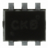
FDY3000NZ Fairchild Semiconductor, FDY3000NZ Datasheet - Page 4

FDY3000NZ
Manufacturer Part Number
FDY3000NZ
Description
MOSFET N-CH DUAL SC89
Manufacturer
Fairchild Semiconductor
Series
PowerTrench®r
Type
Power MOSFETr
Datasheet
1.FDY3000NZ.pdf
(6 pages)
Specifications of FDY3000NZ
Fet Type
2 N-Channel (Dual)
Fet Feature
Logic Level Gate
Rds On (max) @ Id, Vgs
700 mOhm @ 600mA, 4.5V
Drain To Source Voltage (vdss)
20V
Current - Continuous Drain (id) @ 25° C
600mA
Vgs(th) (max) @ Id
1.3V @ 250µA
Gate Charge (qg) @ Vgs
1.1nC @ 4.5V
Input Capacitance (ciss) @ Vds
60pF @ 10V
Power - Max
446mW
Mounting Type
Surface Mount
Package / Case
SC-89-6, SOT-666
Configuration
Dual
Transistor Polarity
N-Channel
Resistance Drain-source Rds (on)
0.7 Ohm @ 4.5 V
Forward Transconductance Gfs (max / Min)
1.8 S
Drain-source Breakdown Voltage
20 V
Gate-source Breakdown Voltage
+/- 12 V
Continuous Drain Current
0.6 A
Power Dissipation
625 mW
Maximum Operating Temperature
+ 150 C
Mounting Style
SMD/SMT
Minimum Operating Temperature
- 55 C
Number Of Elements
2
Polarity
N
Channel Mode
Enhancement
Drain-source On-res
0.7Ohm
Drain-source On-volt
20V
Gate-source Voltage (max)
±12V
Operating Temp Range
-55C to 150C
Operating Temperature Classification
Military
Mounting
Surface Mount
Pin Count
6
Package Type
SC-89
Lead Free Status / RoHS Status
Lead free / RoHS Compliant
Other names
FDY3000NZTR
Available stocks
Company
Part Number
Manufacturer
Quantity
Price
Company:
Part Number:
FDY3000NZ
Manufacturer:
Fairchild Semiconductor
Quantity:
74 306
Typical Characteristics
FDY3000NZ Rev B
0.01
0.1
0.01
10
Figure 9. Maximum Safe Operating Area.
5
4
3
2
1
0
0.1
1
Figure 7. Gate Charge Characteristics.
0.1
0.0001
0
1
I
R
D
DS(ON)
= 600mA
D = 0.5
SINGLE PULSE
R
V
JA
0.2
T
LIMIT
GS
0.1
0.05
0.02
A
= 280
= 25
0.01
= 4.5V
0.2
SINGLE PULSE
o
o
V
C/W
C
DS
, DRAIN-SOURCE VOLTAGE (V)
0.001
Q
1
g
, GATE CHARGE (nC)
0.4
V
DS
1s
DC
= 5V
Figure 11. Transient Thermal Response Curve.
10s
100ms
Thermal characterization performed using the conditions described in Note 1b.
Transient thermal response will change depending on the circuit board design.
0.6
10V
10ms
0.01
10
1ms
15V
0.8
0.1
100
1
t
1
, TIME (sec)
100
90
80
70
60
50
40
30
20
10
30
25
20
15
10
0.0001
0
5
0
0
Figure 8 . Capacitance Characteristics.
1
C
Figure 10. Single Pulse Maximum
rss
0.001
4
V
C
Power Dissipation.
DS
oss
0.01
, DRAIN TO SOURCE VOLTAGE (V)
10
t
8
0.1
1
, TIME (sec)
C
iss
P(pk)
Duty Cycle, D = t
T
1
R
R
J
12
JA
- T
JA
(t) = r(t) * R
100
A
t
=280 °C/W
1
= P * R
t
2
10
www.fairchildsemi.com
SINGLE PULSE
R
JA
T
A
= 280°C/W
16
= 25°C
JA
1
100
JA
(t)
/ t
V
f = 1MHz
2
GS
= 0 V
1000
1000
20


