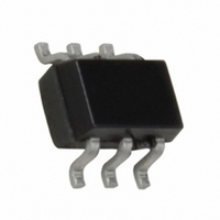
FDG6321C Fairchild Semiconductor, FDG6321C Datasheet - Page 7

FDG6321C
Manufacturer Part Number
FDG6321C
Description
MOSFET N/P-CH DUAL 25V SC70-6
Manufacturer
Fairchild Semiconductor
Datasheet
1.FDG6321C.pdf
(9 pages)
Specifications of FDG6321C
Fet Type
N and P-Channel
Fet Feature
Logic Level Gate
Rds On (max) @ Id, Vgs
450 mOhm @ 500mA, 4.5V
Drain To Source Voltage (vdss)
25V
Current - Continuous Drain (id) @ 25° C
500mA, 410mA
Vgs(th) (max) @ Id
1.5V @ 250µA
Gate Charge (qg) @ Vgs
2.3nC @ 4.5V
Input Capacitance (ciss) @ Vds
50pF @ 10V
Power - Max
300mW
Mounting Type
Surface Mount
Package / Case
SC-70-6, SC-88, SOT-363
Configuration
Dual
Transistor Polarity
N and P-Channel
Resistance Drain-source Rds (on)
0.45 Ohm @ 4.5 V @ N Channel
Forward Transconductance Gfs (max / Min)
1.45 S, 0.9 S
Drain-source Breakdown Voltage
25 V
Gate-source Breakdown Voltage
8 V @ N Channel or - 8 V @ P Channel
Continuous Drain Current
0.5 A @ N Channel or 0.41 A @ P Channel
Power Dissipation
300 mW
Maximum Operating Temperature
+ 150 C
Mounting Style
SMD/SMT
Minimum Operating Temperature
- 55 C
Continuous Drain Current Id
500mA
Drain Source Voltage Vds
25V
On Resistance Rds(on)
450mohm
Rds(on) Test Voltage Vgs
4.5V
Threshold Voltage Vgs Typ
800mV
Rohs Compliant
Yes
Lead Free Status / RoHS Status
Lead free / RoHS Compliant
Other names
FDG6321C
Available stocks
Company
Part Number
Manufacturer
Quantity
Price
Company:
Part Number:
FDG6321C
Manufacturer:
FSC
Quantity:
1 308
Company:
Part Number:
FDG6321C
Manufacturer:
SITRONIX
Quantity:
5 563
Part Number:
FDG6321C
Manufacturer:
FAIRCHILD/ن»™ç«¥
Quantity:
20 000
Typical Electrical Characteristics: P-Channel
0.05
0.01
5
4
3
2
1
0
Figure 17. Gate Charge Characteristics.
0.5
0.1
Figure 19. Maximum Safe Operating Area.
0
3
1
0.1
I = -0.41A
D
SINGLE PULSE
R
0.2
V
T
A
GS
JA
A
= 415°C
= -4.5V
= 25°C
0.4
- V
0.5
DS
Q
, DRAIN-SOURCE VOLTAGE (V)
g
, GATE CHARGE (nC)
1
0.8
2
V
DS
= -5V
5
1.2
-15V
10
-10V
25
1.6
40
50
40
30
20
10
0.0001
0
200
80
30
10
(continued)
5
3
0.1
Figure 18. Capacitance Characteristics.
Figure 20. Single Pulse Maximum Power
f = 1 MHz
V
GS
0.001
= 0 V
0.3
-V
DS
, DRAIN TO SOURCE VOLTAGE (V)
0.01
SINGLE PULSE TIME (SEC)
Dissipation.
1
0.1
2
1
SINGLE PULSE
R
5
JA
T = 25°C
A
=415°C/W
10
10
FDG6321C Rev. D
C iss
C oss
C rss
25
200


