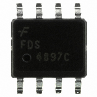
FDS4897C Fairchild Semiconductor, FDS4897C Datasheet - Page 6

FDS4897C
Manufacturer Part Number
FDS4897C
Description
MOSFET N/P-CH 40V 8-SOIC
Manufacturer
Fairchild Semiconductor
Series
PowerTrench®r
Datasheet
1.FDS4897C.pdf
(9 pages)
Specifications of FDS4897C
Fet Type
N and P-Channel
Fet Feature
Logic Level Gate
Rds On (max) @ Id, Vgs
29 mOhm @ 6.2A, 10V
Drain To Source Voltage (vdss)
40V
Current - Continuous Drain (id) @ 25° C
6.2A, 4.4A
Vgs(th) (max) @ Id
3V @ 250µA
Gate Charge (qg) @ Vgs
20nC @ 10V
Input Capacitance (ciss) @ Vds
760pF @ 20V
Power - Max
900mW
Mounting Type
Surface Mount
Package / Case
8-SOIC (3.9mm Width)
Configuration
Dual Dual Drain
Transistor Polarity
N and P-Channel
Resistance Drain-source Rds (on)
0.029 Ohm @ 10 V @ N Channel
Drain-source Breakdown Voltage
40 V
Gate-source Breakdown Voltage
+/- 20 V
Continuous Drain Current
6.2 A @ N Channel or 4.4 A @ P Channel
Power Dissipation
2000 mW
Maximum Operating Temperature
+ 150 C
Mounting Style
SMD/SMT
Minimum Operating Temperature
- 55 C
Lead Free Status / RoHS Status
Lead free / RoHS Compliant
Other names
FDS4897CTR
Available stocks
Company
Part Number
Manufacturer
Quantity
Price
Company:
Part Number:
FDS4897C
Manufacturer:
FSC
Quantity:
30 000
Company:
Part Number:
FDS4897C
Manufacturer:
Fairchild Semiconductor
Quantity:
66 154
Part Number:
FDS4897C
Manufacturer:
FAIRCHILD/ن»™ç«¥
Quantity:
20 000
Company:
Part Number:
FDS4897C-NL
Manufacturer:
FAIRCHILD
Quantity:
50 000
Part Number:
FDS4897C-NL
Manufacturer:
FAIRCHILD/ن»™ç«¥
Quantity:
20 000
Typical Characteristics: Q2 (P-Channel)
FDS4897C Rev C(W)
1.6
1.5
1.4
1.3
1.2
1.1
0.9
0.8
0.7
0.6
Figure 15. On-Resistance Variation with
25
20
15
10
30
25
20
15
10
1
Figure 13. On-Region Characteristics.
5
0
5
0
-50
1.5
Figure 17. Transfer Characteristics.
0
V
V
I
GS
D
GS
= -4.4A
0.5
= - 10V
-25
V
= -10V
DS
= -10V
2
-V
-V
1
T
0
GS
DS
J
, JUNCTION TEMPERATURE (
Temperature.
, DRAIN TO SOURCE VOLTAGE (V)
, GATE TO SOURCE VOLTAGE (V)
-6.0V
1.5
2.5
25
2
50
-4.5V
3
2.5
T
75
A
= -55
3.5
3
-4.0V
o
o
C
100
C)
125
3.5
-3.5V
o
C
4
-3.0V
125
4
25
o
C
150
4.5
4.5
Figure 18. Body Diode Forward Voltage Variation
0.0001
0.001
Figure 14. On-Resistance Variation with
Figure 16. On-Resistance Variation with
0.01
0.14
0.12
0.08
0.06
0.04
0.02
100
with Source Current and Temperature.
0.1
2.6
2.4
2.2
1.8
1.6
1.4
1.2
0.8
0.1
10
1
2
1
0
2
0
Drain Current and Gate Voltage.
V
V
GS
T
GS
A
= 0V
= 25
= - 3.5V
Gate-to-Source Voltage.
0.2
-V
o
5
C
SD
-V
, BODY DIODE FORWARD VOLTAGE (V)
-4.0V
GS
4
, GATE TO SOURCE VOLTAGE (V)
T
T
-I
0.4
A
10
A
D
= 125
= 125
, DRAIN CURRENT (A)
-4.5V
o
o
C
C
0.6
15
6
25
o
-6.0V
C
0.8
20
-55
-10V
o
8
C
www.fairchildsemi.com
I
D
25
1
= -2.2A
10
1.2
30


