NTZD3152PT1G ON Semiconductor, NTZD3152PT1G Datasheet
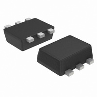
MOSFET 2P-CH 20V 430MA SOT-563

NTZD3152PT1G

Manufacturer Part Number
NTZD3152PT1G
Description
MOSFET 2P-CH 20V 430MA SOT-563
Manufacturer
ON Semiconductor
Datasheet

Specifications of NTZD3152PT1G

Fet Type
2 P-Channel (Dual)
Fet Feature
Logic Level Gate
Rds On (max) @ Id, Vgs
900 mOhm @ 430mA, 4.5V
Drain To Source Voltage (vdss)
20V
Current - Continuous Drain (id) @ 25° C
430mA
Vgs(th) (max) @ Id
1V @ 250µA
Gate Charge (qg) @ Vgs
2.5nC @ 4.5V
Input Capacitance (ciss) @ Vds
175pF @ 16V
Power - Max
250mW
Mounting Type
Surface Mount
Package / Case
SOT-563, SOT-6
Configuration
Dual
Transistor Polarity
P-Channel
Resistance Drain-source Rds (on)
0.9 Ohm @ 4.5 V
Drain-source Breakdown Voltage
20 V
Gate-source Breakdown Voltage
+/- 6 V
Continuous Drain Current
0.43 A
Power Dissipation
280 mW
Maximum Operating Temperature
+ 150 C
Mounting Style
SMD/SMT
Minimum Operating Temperature
- 55 C
Lead Free Status / RoHS Status
Lead free / RoHS Compliant
Other names
NTZD3152PT1GOSTR

Available stocks

Company
Part Number
Manufacturer
Quantity
Price
Part Number:
NTZD3152PT1G
Manufacturer:
ON
Quantity:
4 000
Part Number:
NTZD3152PT1G
Manufacturer:
ON Semiconductor
Quantity:
500
Part Number:
NTZD3152PT1G
Manufacturer:
ON
Quantity:
30 000
Part Number:
NTZD3152PT1G
Manufacturer:
ON
Quantity:
10 000
Part Number:
NTZD3152PT1G
Manufacturer:
ON/安森美
Quantity:
20 000
Part Number:
NTZD3152PT1G
0
Company:
Part Number:
NTZD3152PT1G
Quantity:
326
Company:
Part Number:
NTZD3152PT1G
Quantity:
180
Company:
Part Number:
NTZD3152PT1G
Quantity:
808
NTZD3152P
Small Signal MOSFET
−20 V, −430 mA, Dual P−Channel
with ESD Protection, SOT−563
Features
Applications
Stresses exceeding Maximum Ratings may damage the device. Maximum
Ratings are stress ratings only. Functional operation above the Recommended
Operating Conditions is not implied. Extended exposure to stresses above the
Recommended Operating Conditions may affect device reliability.
1. Surface mounted on FR4 board using 1 in. sq. pad size
© Semiconductor Components Industries, LLC, 2010
March, 2010 − Rev. 2
MAXIMUM RATINGS
THERMAL RESISTANCE RATINGS
Drain−to−Source Voltage
Gate−to−Source Voltage
Continuous Drain Current
Power Dissipation
Continuous Drain Current
Power Dissipation
Pulsed Drain Current
Operating Junction and Storage Temperature
Source Current (Body Diode)
Lead Temperature for Soldering Purposes
Junction−to−Ambient – Steady State (Note 1)
Junction−to−Ambient – t v 5 s (Note 1)
Low R
Low Threshold Voltage
ESD Protected Gate
Small Footprint 1.6 x 1.6 mm
These are Pb−Free Devices
Load/Power Switches
Power Supply Converter Circuits
Battery Management
Cell Phones, Digital Cameras, PDAs, Pagers, etc.
(Cu. area = 1.127 in. sq. [1 oz.] including traces).
(Note 1)
(Note 1)
(Note 1)
(Note 1)
(1/8″ from case for 10 s)
DS(on)
Improving System Efficiency
Parameter
Parameter
(T
J
= 25°C unless otherwise noted.)
t v 5 s
Steady
State
Steady State
t
p
t v 5 s
= 10 ms
T
T
T
T
A
A
A
A
= 25°C
= 85°C
= 25°C
= 85°C
Symbol
Symbol
V
T
R
V
I
T
P
P
DSS
STG
T
I
I
DM
I
qJA
GS
D
D
S
J
D
D
L
,
−55 to
Value
−430
−310
−455
−328
−750
−350
±6.0
Max
−20
250
280
150
260
500
447
1
°C/W
Unit
Unit
mW
mW
mA
mA
mA
mA
°C
°C
V
V
G
†For information on tape and reel specifications,
NTZD3152PT1G
NTZD3152PT1H
NTZD3152PT5G
NTZD3152PT5H
including part orientation and tape sizes, please
refer to our Tape and Reel Packaging Specifications
Brochure, BRD8011/D.
1
V
−20 V
(BR)DSS
(Note: Microdot may be in either location)
Device
6
CASE 463A
SOT−563−6
D
G
S
2
1
1
TU
M
G
ORDERING INFORMATION
1
2
3
D
S
1
1
1
http://onsemi.com
PINOUT: SOT−563
0.5 W @ −4.5 V
0.6 W @ −2.5 V
1.0 W @ −1.8 V
R
= Specific Device Code
= Date Code
= Pb−Free Package
DS(on)
(Pb−Free)
(Pb−Free)
SOT−563
SOT−563
Package
Top View
P−Channel
MOSFET
MARKING DIAGRAM
Typ
Publication Order Number:
G
2
1
4000 / Tape & Reel
8000 / Tape & Reel
TU M G
Shipping
G
NTZD3152P/D
6
5
4
−430 mA
D
S
I
D
2
2
S
D
G
Max
2
1
2

Related parts for NTZD3152PT1G

NTZD3152PT1G Summary of contents

Page 1

... 260 °C L Symbol Max Unit Device 500 °C/W R NTZD3152PT1G qJA 447 NTZD3152PT1H NTZD3152PT5G NTZD3152PT5H †For information on tape and reel specifications, including part orientation and tape sizes, please refer to our Tape and Reel Packaging Specifications Brochure, BRD8011/D. 1 http://onsemi.com R Typ I Max ...

Page 2

ELECTRICAL CHARACTERISTICS Parameter OFF CHARACTERISTICS Drain−to−Source Breakdown Voltage Drain−to−Source Breakdown Voltage Temperature Coefficient Zero Gate Voltage Drain Current Gate−to−Source Leakage Current ON CHARACTERISTICS (Note 2) Gate Threshold Voltage Negative Threshold Temperature Coefficient Drain−to−Source On Resistance Forward Transconductance CHARGES AND CAPACITANCES ...

Page 3

TYPICAL PERFORMANCE CURVES 25° − −1 −1 0.6 −1.4 V 0.4 −1.2 V 0.2 − −V , ...

Page 4

TYPICAL PERFORMANCE CURVES 250 200 C 150 ISS 100 C OSS 50 C RSS GATE−TO−SOURCE OR DRAIN−TO−SOURCE VOLTAGE (VOLTS) Figure 7. Capacitance Variation 100 t d(off ...

Page 5

... Pb−Free strategy and soldering details, please download the ON Semiconductor Soldering and Mounting Techniques Reference Manual, SOLDERRM/D. ON Semiconductor and are registered trademarks of Semiconductor Components Industries, LLC (SCILLC). SCILLC reserves the right to make changes without further notice to any products herein ...

Related keywords