SI1539DL-T1-E3 Vishay, SI1539DL-T1-E3 Datasheet - Page 2
SI1539DL-T1-E3
Manufacturer Part Number
SI1539DL-T1-E3
Description
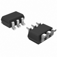
MOSFET N/P-CH 30V SC70-6
Manufacturer
Vishay
Series
TrenchFET®r
Datasheets
1.SI1539DL-T1-E3.pdf
(8 pages)
2.SI1539DL-T1-E3.pdf
(8 pages)
3.SI1539DL-T1-E3.pdf
(12 pages)
Specifications of SI1539DL-T1-E3
Transistor Polarity
N and P-Channel
Fet Type
N and P-Channel
Fet Feature
Logic Level Gate
Rds On (max) @ Id, Vgs
480 mOhm @ 590mA, 10V
Drain To Source Voltage (vdss)
30V
Current - Continuous Drain (id) @ 25° C
540mA, 420mA
Vgs(th) (max) @ Id
1V @ 250µA
Gate Charge (qg) @ Vgs
1.4nC @ 10V
Power - Max
270mW
Mounting Type
Surface Mount
Package / Case
SC-70-6, SC-88, SOT-363
Minimum Operating Temperature
- 55 C
Configuration
Dual
Resistance Drain-source Rds (on)
0.48 Ohm @ 10 V @ N Channel
Drain-source Breakdown Voltage
30 V
Gate-source Breakdown Voltage
+/- 20 V
Continuous Drain Current
0.54 A @ N Channel or 0.42 A @ P Channel
Power Dissipation
270 mW
Maximum Operating Temperature
+ 150 C
Mounting Style
SMD/SMT
Continuous Drain Current Id
630mA
Drain Source Voltage Vds
30V
On Resistance Rds(on)
480mohm
Rds(on) Test Voltage Vgs
10V
Threshold Voltage Vgs Typ
1V
Module Configuration
Dual
Rohs Compliant
Yes
Lead Free Status / RoHS Status
Lead free / RoHS Compliant
Lead Free Status / RoHS Status
Lead free / RoHS Compliant, Lead free / RoHS Compliant
Other names
SI1539DL-T1-E3TR
Available stocks
Company
Part Number
Manufacturer
Quantity
Price

Part Number:
SI1539DL-T1-E3
Manufacturer:
VISHAY/威世
Quantity:
20 000


Notes
a.
b.
www.vishay.com
2-2
Si1539DL
Vishay Siliconix
SPECIFICATIONS (T
Static
Gate Threshold Voltage
Gate-Body Leakage
Zero Gate Voltage Drain Current
On-State Drain Current
Drain-Source On-State Resistance
Forward Transconductance
Diode Forward Voltage
Dynamic
Total Gate Charge
Gate-Source Charge
Gate-Drain Charge
Turn-On Delay Time
Rise Time
Turn-Off Delay Time
Fall Time
Source-Drain
Source-Drain
Reverse Recovery Time
Pulse test; pulse width v 300 ms, duty cycle v 2%.
Guaranteed by design, not subject to production testing.
b
Parameter
a
a
a
a
J
= 25_C UNLESS OTHERWISE NOTED)
Symbol
V
r
I
DS(on)
t
I
t
I
GS(th)
D(on)
V
Q
Q
d(off)
d(on)
GSS
DSS
g
Q
t
SD
t
t
rr
fs
gs
gd
r
f
g
V
V
I ^ -0.5 A, V
I
DS
D
V
I
DS
V
D
^ -0.5 A, V
DS
DS
= -15 V, V
^ 0.5 A, V
I
= 15 V, V
I
F
F
V
V
V
V
V
= -24 V, V
V
= 24 V, V
= -0.23 A, di/dt = 100 A/ms
V
V
V
V
I
V
GS
V
= 0.23 A, di/dt = 100 A/ms
DS
V
DS
V
GS
I
S
V
DS
DS
S
DS
DS
DD
DS
GS
DS
GS
DD
DS
= -0.23 A, V
= 0.23 A, V
p -5 V, V
= -10 V, I
= -15 V, I
= V
= 0 V, V
= -4.5 V, I
= V
= -24 V, V
w 5 V, V
= 10 V, I
= 15 V, I
= -15 V, R
= 24 V, V
= 4.5 V, I
= 15 V, R
N-Channel
N-Channel
P-Channel
N-Channel
P-Channel
P-Channel
Test Condition
GS
GS
GEN
GEN
GS
GS
GS
GS
, I
, I
= -10 V, I
= 10 V, I
GS
= 0 V, T
D
= 10 V, R
= -10 V, R = 6 W
= -10 V, R
D
= 0 V, T
D
D
D
D
GS
GS
= -250 mA
D
D
GS
GS
= 250 mA
L
GS
= 0.59 A
GS
= 0.59 A
= -0.42 A
L
= "20 V
= -0.42 A
= 0.2 A
= -0.2 A
= 30 W
= 30 W
= 10 V
= -10 V
"
= 0 V
= 0 V
= 0 V
= 0 V
D
J
D
J
W
= 85_C
= 0.59 A
G
W
= 85_C
= -0.42 A
G
= 6 W
= 6 W
N-Ch
P-Ch
N-Ch
P-Ch
N-Ch
P-Ch
N-Ch
P-Ch
N-Ch
P-Ch
N-Ch
P-Ch
N-Ch
P-Ch
N-Ch
P-Ch
N-Ch
P-Ch
N-Ch
P-Ch
N-Ch
P-Ch
N-Ch
P-Ch
N-Ch
P-Ch
N-Ch
P-Ch
N-Ch
P-Ch
N-Ch
P-Ch
N-Ch
P-Ch
Min
-1.0
-1.0
1.0
1.0
S-21374—Rev. B, 12-Aug-02
0.410
0.800
0.600
-0.86
Typ
0.75
0.86
0.24
0.21
0.08
0.17
1.5
0.5
0.8
0.9
15
20
Document Number: 71250
5
4
8
8
8
5
7
7
"100
"100
Max
0.480
0.940
0.700
1.700
-1.2
1.2
1.4
1.4
-1
-5
10
10
15
15
15
10
15
15
30
40
1
5
Unit
nA
m
mA
nC
ns
W
W
V
A
S
V
Related parts for SI1539DL-T1-E3
Image
Part Number
Description
Manufacturer
Datasheet
Request
R

Part Number:
Description:
Complementary 30-v D-s Mosfet
Manufacturer:
Vishay
Datasheet:
Part Number:
Description:
N/P-Ch SC-70-6 (SOT-363) 30V 480/940mohm @ 10V
Manufacturer:
Vishay

Part Number:
Description:
MOSFET 30 0.63/0.45
Manufacturer:
Vishay/Siliconix
Datasheet:
Part Number:
Description:
357-036-542-201 CARDEDGE 36POS DL .156 BLK LOPRO
Manufacturer:
Vishay
Datasheet:
Part Number:
Description:
357-036-542-201 CARDEDGE 36POS DL .156 BLK LOPRO
Manufacturer:
Vishay
Datasheet:
Part Number:
Description:
357-036-542-201 CARDEDGE 36POS DL .156 BLK LOPRO
Manufacturer:
Vishay
Datasheet:
Part Number:
Description:
357-036-542-201 CARDEDGE 36POS DL .156 BLK LOPRO
Manufacturer:
Vishay
Datasheet:
Part Number:
Description:
357-036-542-201 CARDEDGE 36POS DL .156 BLK LOPRO
Manufacturer:
Vishay
Datasheet:
Part Number:
Description:
357-036-542-201 CARDEDGE 36POS DL .156 BLK LOPRO
Manufacturer:
Vishay
Datasheet:
Part Number:
Description:
357-036-542-201 CARDEDGE 36POS DL .156 BLK LOPRO
Manufacturer:
Vishay
Datasheet:
Part Number:
Description:
357-036-542-201 CARDEDGE 36POS DL .156 BLK LOPRO
Manufacturer:
Vishay
Datasheet:
Part Number:
Description:
357-036-542-201 CARDEDGE 36POS DL .156 BLK LOPRO
Manufacturer:
Vishay
Datasheet:
Part Number:
Description:
357-036-542-201 CARDEDGE 36POS DL .156 BLK LOPRO
Manufacturer:
Vishay
Datasheet:
Part Number:
Description:
357-036-542-201 CARDEDGE 36POS DL .156 BLK LOPRO
Manufacturer:
Vishay
Datasheet:
Part Number:
Description:
357-036-542-201 CARDEDGE 36POS DL .156 BLK LOPRO
Manufacturer:
Vishay
Datasheet: