FDS9953A Fairchild Semiconductor, FDS9953A Datasheet
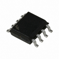
MOSFET P-CH DUAL 30V 2.9A 8SOIC

FDS9953A

Manufacturer Part Number
FDS9953A
Description
MOSFET P-CH DUAL 30V 2.9A 8SOIC
Manufacturer
Fairchild Semiconductor
Series
PowerTrench®r
Datasheet

Specifications of FDS9953A

Fet Type
2 P-Channel (Dual)
Fet Feature
Logic Level Gate
Rds On (max) @ Id, Vgs
130 mOhm @ 1A, 10V
Drain To Source Voltage (vdss)
30V
Current - Continuous Drain (id) @ 25° C
2.9A
Vgs(th) (max) @ Id
3V @ 250µA
Gate Charge (qg) @ Vgs
3.5nC @ 10V
Input Capacitance (ciss) @ Vds
185pF @ 15V
Power - Max
900mW
Mounting Type
Surface Mount
Package / Case
8-SOIC (3.9mm Width)
Configuration
Dual Dual Drain
Transistor Polarity
P-Channel
Resistance Drain-source Rds (on)
0.13 Ohm @ 10 V
Forward Transconductance Gfs (max / Min)
4 S
Drain-source Breakdown Voltage
30 V
Gate-source Breakdown Voltage
+/- 25 V
Continuous Drain Current
2.9 A
Power Dissipation
2000 mW
Maximum Operating Temperature
+ 150 C
Mounting Style
SMD/SMT
Minimum Operating Temperature
- 55 C
Lead Free Status / RoHS Status
Lead free / RoHS Compliant

Available stocks

Company
Part Number
Manufacturer
Quantity
Price
Part Number:
FDS9953A
Manufacturer:
FSC
Quantity:
50 000
Part Number:
FDS9953A
Manufacturer:
FSC
Quantity:
60 000
Part Number:
FDS9953A
Manufacturer:
FAIRCHILD/仙童
Quantity:
20 000
Part Number:
FDS9953A-NL
Manufacturer:
FAIRCHILD
Quantity:
12 651
Part Number:
FDS9953A-NL
Manufacturer:
FAIRCHILD/仙童
Quantity:
20 000
FDS9953A
Dual 30V P-Channel PowerTrench MOSFET
General Description
This P -Channel MOSFET is a rugged gate version of
Fairchild Semiconductor’s advanced PowerTrench
process. It has been optimized for power management
applications requiring a wide range of gave drive
voltage ratings (4.5V – 25V).
Applications
2001 Fairchild Semiconductor Corporation
Absolute Maximum Ratings
Symbol
V
V
I
P
T
Thermal Characteristics
R
R
Package Marking and Ordering Information
D
D
J
DSS
GSS
, T
JA
J C
Device Marking
Power management
Load switch
Battery protection
STG
FDS9953A
SO-8
Drain-Source Voltage
Gate-Source Voltage
Drain Current
Power Dissipation for Dual Operation
Power Dissipation for Single Operation
Operating and Storage Junction Temperature Range
Thermal Resistance, Junction-to-Ambient
Thermal Resistance, Junction-to-Case
Pin 1
D
D2
D
D2
SO-8
D
D1
– Continuous
– Pulsed
FDS9953A
D
Device
D1
Parameter
S2
S
G2
S
S1
S
G1
T
G
A
=25
o
C unless otherwise noted
Reel Size
13’’
(Note 1a)
(Note 1a)
(Note 1b)
(Note 1c)
(Note 1a)
(Note 1)
Features
–2.9 A, –30 V
Low gate charge (2.5nC typical)
Fast switching speed
High performance trench technology for extremely
low R
High power and current handling capability
DS(ON)
5
6
7
8
Tape width
–55 to +150
Q1
Q2
12mm
R
R
Ratings
DS(ON)
DS(ON)
–30
1.6
0.9
78
40
2.9
25
10
2
1
= 130 m @ V
= 200 m @ V
4
3
2
1
May 2001
FDS9953A Rev B(W)
2500 units
GS
GS
Quantity
= –10 V
= –4.5 V
Units
C/W
C/W
W
V
V
A
C

Related parts for FDS9953A

FDS9953A Summary of contents

Page 1

... C unless otherwise noted A (Note 1a) (Note 1a) (Note 1b) (Note 1c) (Note 1a) (Note 1) Reel Size 13’’ May 2001 R = 130 –10 V DS(ON 200 –4.5 V DS(ON Ratings Units – 2 1.6 1 0.9 –55 to +150 C 78 C/W 40 C/W Tape width Quantity 12mm 2500 units FDS9953A Rev B(W) ...

Page 2

... GEN V = – – – –1.3 A (Note –1.25A /dt = 100A Min Typ Max Units –30 V –23 mV/ C –2 A –100 nA 100 nA –1 –1.8 –3 mV 130 m 137 200 142 200 202 310 –5 A –1 185 4 2.5 3.5 nC 0.8 nC 0.9 nC –1.2 A –0.8 1 100 nS FDS9953A Rev B(W) ...

Page 3

... Scale letter size paper 2. Pulse Test: Pulse Width < 300 s, Duty Cycle < 2.0% is determined by the user's board design 125°C/W when mounted 0.02 in pad copper c) 135°C/W when mounted on a minimum pad. FDS9953A Rev B(W) ...

Page 4

... Figure 6. Body Diode Forward Voltage Variation with Source Current and Temperature. -4.0V -4.5V -5.0V -6.0V -10V DRAIN CURRENT ( -0 125 GATE TO SOURCE VOLTAGE (V) GS Gate-to-Source Voltage 125 -55 C 0.2 0.4 0.6 0 BODY DIODE FORWARD VOLTAGE (V) SD FDS9953A Rev B( 1.4 ...

Page 5

... Thermal characterization performed using the conditions described in Note 1c. Transient thermal response will change depending on the circuit board design 1MHz ISS C OSS C RSS DRAIN TO SOURCE VOLTAGE (V) DS SINGLE PULSE R = 135°C 25°C A 0.01 0 TIME (sec) 1 Power Dissipation. R ( 135 °C/W JA P(pk ( Duty Cycle 100 FDS9953A Rev B(W) 30 100 2 1000 ...

Page 6

... TRADEMARKS The following are registered and unregistered trademarks Fairchild Semiconductor owns or is authorized to use and is not intended exhaustive list of all such trademarks. ACEx™ FAST Bottomless™ FASTr™ CoolFET™ FRFET™ CROSSVOLT™ GlobalOptoisolator™ GTO™ DenseTrench™ ...

Related keywords