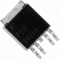
FDD8424H Fairchild Semiconductor, FDD8424H Datasheet

FDD8424H
Specifications of FDD8424H
Available stocks
Related parts for FDD8424H
FDD8424H Summary of contents
Page 1
... Thermal Resistance, Junction to Case, Single Operation for Q2 θJC Package Marking and Ordering Information Device Marking Device FDD8424H FDD8424H ©2007 Fairchild Semiconductor Corporation FDD8424H Rev.C ® MOSFET General Description These dual N and P-Channel enhancement MOSFETs are produced using Fairchild Semiconductor’s = 9.0A D advanced PowerTrench- process that has been especially = 7 ...
Page 2
... Turn-Off Delay Time d(off) t Fall Time f Q Total Gate Charge g(TOT) Q Gate to Source Charge gs Q Gate to Drain “Miller” Charge gd ©2007 Fairchild Semiconductor Corporation FDD8424H Rev 25°C unless otherwise noted J Test Conditions I = 250µ -250µ 250µA, referenced to 25°C ...
Page 3
... Pulse Test: Pulse Width < 300µs, Duty cycle < 2.0%. 3. Starting T = 25°C, N-ch 0.3mH 14A ©2007 Fairchild Semiconductor Corporation FDD8424H Rev 25°C unless otherwise noted J Test Conditions ...
Page 4
... T J Figure 3. Normalized On -Resistance vs Junction Temperature 60 µ PULSE DURATION = 80 s DUTY CYCLE = 0.5%MAX 150 1.5 2.0 2.5 3 GATE TO SOURCE VOLTAGE (V) GS Figure 5. Transfer Characteristics ©2007 Fairchild Semiconductor Corporation FDD8424H Rev 25°C unless otherwise noted 4.0V GS µ 3. 3. 100 125 150 0. - ...
Page 5
... T = MAX RATED 4.1 C/W θ 0 DRAIN to SOURCE VOLTAGE (V) DS Figure 11. Forward Bias Safe Operating Area ©2007 Fairchild Semiconductor Corporation FDD8424H Rev 25°C unless otherwise noted J 2000 1000 V = 20V DD = 25V 100 Figure 10. Maximum Continuous Drain 10000 10us 100us 1000 100 1ms 10ms ...
Page 6
... Typical Characteristics (Q1 N-Channel DUTY CYCLE-DESCENDING ORDER D = 0.5 0.2 0.1 0.05 0.02 0.1 0.01 SINGLE PULSE 0. 4.1 C/W θ JC 0.005 - ©2007 Fairchild Semiconductor Corporation FDD8424H Rev 25°C unless otherwise noted RECTANGULAR PULSE DURATION (s) Figure 13. Transient Thermal Response Curve NOTES: DUTY FACTOR PEAK ...
Page 7
... Fairchild Semiconductor Corporation FDD8424H Rev.C 7 www.fairchildsemi.com ...
Page 8
... Junction Temperature 40 µ PULSE DURATION = 80 s DUTY CYCLE = 0.5%MAX - 150 GATE TO SOURCE VOLTAGE (V) GS Figure 18. Transfer Characteristics ©2007 Fairchild Semiconductor Corporation FDD8424H Rev 25°C unless otherwise noted J µ PULSE DURATION = 80 s DUTY CYCLE = 0.5%MAX V = -4. - -3. - Figure 15. Normalized on-Resistance vs Drain 160 120 50 75 ...
Page 9
... LIMITED BY r ds(on) 1 SINGLE PULSE T = MAX RATED 3.5 C/W θ 0 DRAIN to SOURCE VOLTAGE (V) DS Figure 24 . Forward Bias Safe Operating Area ©2007 Fairchild Semiconductor Corporation FDD8424H Rev 25°C unless otherwise noted J 2000 1000 V = -20V -25V DD 100 100 10000 10us 100us 1000 1ms ...
Page 10
... Typical Characteristics (Q2 P-Channel DUTY CYCLE-DESCENDING ORDER D = 0.5 0.2 0.1 0.05 0.02 0.1 0.01 SINGLE PULSE 0. 3.5 θ JC 0.005 - ©2007 Fairchild Semiconductor Corporation FDD8424H Rev 25°C unless otherwise noted J C RECTANGULAR PULSE DURATION (s) Figure 26. Transient Thermal Response Curve NOTES: DUTY FACTOR PEAK T ...
Page 11
... Fairchild Semiconductor Corporation FDD8424H Rev.C 11 www.fairchildsemi.com ...
Page 12
... Product Status Advance Information Formative or In Design Preliminary First Production No Identification Needed Full Production Obsolete Not In Production ©2007 Fairchild Semiconductor Corporation FDD8424H Rev.C HiSeC™ Programmable Active Droop™ ® i-Lo™ QFET ImpliedDisconnect™ QS™ IntelliMAX™ QT Optoelectronics™ ISOPLANAR™ ...


