NTJD4152PT1G ON Semiconductor, NTJD4152PT1G Datasheet - Page 2
NTJD4152PT1G
Manufacturer Part Number
NTJD4152PT1G
Description
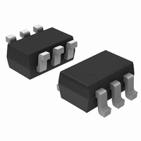
MOSFET 2P-CH 20V 880MA SOT-363
Manufacturer
ON Semiconductor
Type
Small Signalr
Specifications of NTJD4152PT1G
Fet Type
2 P-Channel (Dual)
Fet Feature
Logic Level Gate
Rds On (max) @ Id, Vgs
260 mOhm @ 880mA, 4.5V
Drain To Source Voltage (vdss)
20V
Current - Continuous Drain (id) @ 25° C
880mA
Vgs(th) (max) @ Id
450mV @ 250µA
Gate Charge (qg) @ Vgs
2.2nC @ 4.5V
Input Capacitance (ciss) @ Vds
155pF @ 20V
Power - Max
272mW
Mounting Type
Surface Mount
Package / Case
SC-70-6, SC-88, SOT-363
Configuration
Dual
Transistor Polarity
P-Channel
Resistance Drain-source Rds (on)
0.26 Ohm @ 4.5 V
Forward Transconductance Gfs (max / Min)
3 S
Drain-source Breakdown Voltage
20 V
Gate-source Breakdown Voltage
+/- 12 V
Continuous Drain Current
0.88 A
Power Dissipation
272 mW
Maximum Operating Temperature
+ 150 C
Mounting Style
SMD/SMT
Minimum Operating Temperature
- 55 C
Module Configuration
Dual
Continuous Drain Current Id
880mA
Drain Source Voltage Vds
-20V
On Resistance Rds(on)
215mohm
Rds(on) Test Voltage Vgs
-4.5V
Rohs Compliant
Yes
Number Of Elements
2
Polarity
P
Channel Mode
Enhancement
Drain-source On-res
0.26Ohm
Drain-source On-volt
20V
Gate-source Voltage (max)
±12V
Operating Temp Range
-55C to 150C
Operating Temperature Classification
Military
Mounting
Surface Mount
Pin Count
6
Package Type
SC-88
Lead Free Status / RoHS Status
Lead free / RoHS Compliant
Other names
NTJD4152PT1GOSTR
Available stocks
Company
Part Number
Manufacturer
Quantity
Price
Company:

Part Number:
NTJD4152PT1G
Manufacturer:
ON
Quantity:
36 000
Company:
Part Number:
NTJD4152PT1G
Manufacturer:
ON
Quantity:
3 000
Company:
Part Number:
NTJD4152PT1G
Manufacturer:
ON
Quantity:
30 000
Part Number:
NTJD4152PT1G
Manufacturer:
ON/安森美
Quantity:
20 000


3. Pulse Test: pulse width ≤ 300ms, duty cycle ≤ 2%.
4. Switching characteristics are independent of operating junction temperatures.
ELECTRICAL CHARACTERISTICS
OFF CHARACTERISTICS
ON CHARACTERISTICS (Note 3)
CHARGES AND CAPACITANCES
SWITCHING CHARACTERISTICS (Note 4)
DRAIN-SOURCE DIODE CHARACTERISTICS
Drain-to-Source Breakdown Voltage
Zero Gate Voltage Drain Current
Gate-to-Source Leakage Current
Gate Threshold Voltage
Drain-to-Source On Resistance
Forward Transconductance
Input Capacitance
Output Capacitance
Reverse Transfer Capacitance
Total Gate Charge
Gate-to-Source Charge
Gate-to-Drain Charge
Turn-On Delay Time
Rise Time
Turn-Off Delay Time
Fall Time
Forward Diode Voltage
Parameter
V
(T
Symbol
Q
V
R
t
(BR)DSS
t
C
C
d(OFF)
GS(TH)
C
I
I
G(TOT)
Q
Q
d(ON)
DS(on)
V
J
g
GSS
DSS
OSS
=25°C unless otherwise stated)
RSS
ISS
t
FS
GS
GD
t
SD
r
f
V
GS
= 0 V, V
http://onsemi.com
V
V
V
V
V
I
V
V
V
S
GS
GS
V
V
V
V
GS
GS
GS
NTJD4152P
DS
I
GS
GS
= -0.48 A
DS
D
GS
GS
DS
= -4.5 V, V
= -4.5 V, V
= -0.5 A, R
= -4.5 V, I
= -2.5 V, I
= -1.8 V, I
= -10 V, I
= 0 V,
Test Condition
= V
= 0 V, V
= 0 V, I
= 0 V, V
= 0 V, f = 1.0 MHz,
DS
V
I
D
DS
DS
2
= -0.88 A
= -16 V
, ID = -250 mA
= -20 V
D
GS
GS
D
= -250 mA
D
D
D
DS
DD
G
= -0.88 A
= ±4.5 V
= -0.88 A
= -0.71 A
= -0.20 A
= ±12 V
= 20 W
= -10 V,
= -10 V,
T
T
T
T
J
J
J
J
= 125°C
= 125°C
= 25°C
= 25°C
-0.45
Min
-20
-0.66
0.03
0.65
13.5
-0.8
Typ
215
345
600
155
1.0
6.0
3.0
2.2
0.5
5.8
6.5
3.5
25
18
1000
Max
-1.2
260
500
1.0
5.0
1.0
Unit
mW
mA
mA
nC
pF
ns
V
V
S
V
Related parts for NTJD4152PT1G
Image
Part Number
Description
Manufacturer
Datasheet
Request
R

Part Number:
Description:
ON Semiconductor [VOLTAGE REGULATOR]
Manufacturer:
ON Semiconductor
Datasheet:
Part Number:
Description:
357-036-542-201 CARDEDGE 36POS DL .156 BLK LOPRO
Manufacturer:
ON Semiconductor
Datasheet:
Part Number:
Description:
357-036-542-201 CARDEDGE 36POS DL .156 BLK LOPRO
Manufacturer:
ON Semiconductor
Datasheet:
Part Number:
Description:
357-036-542-201 CARDEDGE 36POS DL .156 BLK LOPRO
Manufacturer:
ON Semiconductor
Datasheet:
Part Number:
Description:
357-036-542-201 CARDEDGE 36POS DL .156 BLK LOPRO
Manufacturer:
ON Semiconductor
Datasheet:
Part Number:
Description:
357-036-542-201 CARDEDGE 36POS DL .156 BLK LOPRO
Manufacturer:
ON Semiconductor
Datasheet:
Part Number:
Description:
357-036-542-201 CARDEDGE 36POS DL .156 BLK LOPRO
Manufacturer:
ON Semiconductor
Datasheet:
Part Number:
Description:
357-036-542-201 CARDEDGE 36POS DL .156 BLK LOPRO
Manufacturer:
ON Semiconductor
Datasheet:
Part Number:
Description:
357-036-542-201 CARDEDGE 36POS DL .156 BLK LOPRO
Manufacturer:
ON Semiconductor
Datasheet:
Part Number:
Description:
357-036-542-201 CARDEDGE 36POS DL .156 BLK LOPRO
Manufacturer:
ON Semiconductor
Datasheet:
Part Number:
Description:
357-036-542-201 CARDEDGE 36POS DL .156 BLK LOPRO
Manufacturer:
ON Semiconductor
Datasheet:
Part Number:
Description:
Manufacturer:
ON Semiconductor
Datasheet:
Part Number:
Description:
Manufacturer:
ON Semiconductor
Datasheet:
Part Number:
Description:
Manufacturer:
ON Semiconductor
Datasheet: