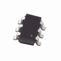
ZXMP6A17E6TA Diodes Zetex, ZXMP6A17E6TA Datasheet - Page 4

ZXMP6A17E6TA
Manufacturer Part Number
ZXMP6A17E6TA
Description
MOSFET P-CH 60V 3A SOT-23-6
Manufacturer
Diodes Zetex
Type
Power MOSFETr
Datasheet
1.ZXMP6A17E6TA.pdf
(8 pages)
Specifications of ZXMP6A17E6TA
Fet Type
MOSFET P-Channel, Metal Oxide
Fet Feature
Logic Level Gate
Rds On (max) @ Id, Vgs
125 mOhm @ 2.3A, 10V
Drain To Source Voltage (vdss)
60V
Current - Continuous Drain (id) @ 25° C
2.3A
Vgs(th) (max) @ Id
1V @ 250µA
Gate Charge (qg) @ Vgs
17.7nC @ 10V
Input Capacitance (ciss) @ Vds
637pF @ 30V
Power - Max
1.1W
Mounting Type
Surface Mount
Package / Case
SOT-23-6
Number Of Elements
1
Polarity
P
Channel Mode
Enhancement
Drain-source On-res
0.125Ohm
Drain-source On-volt
60V
Gate-source Voltage (max)
±20V
Drain Current (max)
3A
Power Dissipation
1.92W
Output Power (max)
Not RequiredW
Frequency (max)
Not RequiredMHz
Noise Figure
Not RequireddB
Power Gain
Not RequireddB
Drain Efficiency
Not Required%
Operating Temp Range
-55C to 150C
Operating Temperature Classification
Military
Mounting
Surface Mount
Pin Count
6
Package Type
SOT-23
Continuous Drain Current
3A
Lead Free Status / RoHS Status
Lead free / RoHS Compliant
Other names
ZXMP6A17E6TR
Available stocks
Company
Part Number
Manufacturer
Quantity
Price
Company:
Part Number:
ZXMP6A17E6TA
Manufacturer:
ZETEX
Quantity:
21 000
Company:
Part Number:
ZXMP6A17E6TA
Manufacturer:
NS
Quantity:
41
Part Number:
ZXMP6A17E6TA
Manufacturer:
ZETEX/DIODES
Quantity:
20 000
Electrical Characteristics
OFF CHARACTERISTICS
Drain-Source Breakdown Voltage
Zero Gate Voltage Drain Current
Gate-Source Leakage
ON CHARACTERISTICS
Gate Threshold Voltage
Static Drain-Source On-Resistance (Note 7)
Forward Transconductance (Notes 7 & 8)
Diode Forward Voltage (Note 7)
Reverse recovery time (Note 8)
Reverse recovery charge (Note 8)
DYNAMIC CHARACTERISTICS (Note 8)
Input Capacitance
Output Capacitance
Reverse Transfer Capacitance
Total Gate Charge (Note 9)
Total Gate Charge (Note 9)
Gate-Source Charge (Note 9)
Gate-Drain Charge (Note 9)
Turn-On Delay Time (Note 9)
Turn-On Rise Time (Note 9)
Turn-Off Delay Time (Note 9)
Turn-Off Fall Time (Note 9)
Notes:
ZXMP6A17E6
Document Number: DS33589 Rev. 2 - 2
7. Measured under pulsed conditions. Pulse width ≤ 300μs; duty cycle ≤ 2%
8. For design aid only, not subject to production testing.
9. Switching characteristics are independent of operating junction temperatures.
Characteristic
@T
A
= 25°C unless otherwise specified
Symbol
R
BV
V
DS (ON)
t
t
I
I
C
V
C
C
GS(th)
Q
Q
D(on)
D(off)
DSS
GSS
Q
Q
Q
g
t
oss
t
t
SD
rss
DSS
rr
iss
fs
gs
gd
r
f
rr
g
g
www.diodes.com
Min
-1.0
4 of 8
-60
⎯
⎯
⎯
⎯
⎯
⎯
⎯
⎯
⎯
⎯
⎯
⎯
⎯
⎯
⎯
⎯
⎯
0.100
0.130
-0.85
25.1
27.2
17.7
26.2
11.3
Typ
637
4.7
9.8
1.6
4.4
2.6
3.4
70
53
⎯
⎯
⎯
⎯
0.125
0.190
±100
-0.95
Max
-1.0
-3.0
⎯
⎯
⎯
⎯
⎯
⎯
⎯
⎯
⎯
⎯
⎯
⎯
⎯
⎯
⎯
Diodes Incorporated
A Product Line of
Unit
μA
nA
nC
nC
nC
nC
nC
ns
pF
pF
pF
ns
ns
ns
ns
Ω
V
V
S
V
I
V
V
I
V
V
V
I
I
V
f = 1MHz
V
V
V
I
D
D
S
F
D
DS
GS
GS
GS
DS
DS
GS
GS
DD
= -1.7A, di/dt = 100A/μs
= -250μA, V
= -250μA, V
= -2A, V
= -1A, R
= -60V, V
= ±20V, V
= -10V, I
= -4.5V, I
= -15V, I
= -30V, V
= -5.0V
= -10V
= -30V, V
Test Condition
GS
G
ZXMP6A17E6
≅ 6.0Ω
D
D
= 0V
D
GS
GS
GS
GS
DS
DS
= -2.3A
= -2.3A
= -1.9A
= 0V
= 0V
= -10V
= 0V
= V
= 0V
V
I
© Diodes Incorporated
D
December 2010
DS
= -2.3A
GS
= -30V


