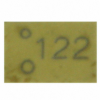
FDZ191P Fairchild Semiconductor, FDZ191P Datasheet - Page 2

FDZ191P
Manufacturer Part Number
FDZ191P
Description
MOSFET P-CH 20V 3A 6WLCSP
Manufacturer
Fairchild Semiconductor
Series
PowerTrench®r
Datasheet
1.FDZ191P.pdf
(7 pages)
Specifications of FDZ191P
Fet Type
MOSFET P-Channel, Metal Oxide
Fet Feature
Logic Level Gate
Rds On (max) @ Id, Vgs
85 mOhm @ 1A, 4.5V
Drain To Source Voltage (vdss)
20V
Current - Continuous Drain (id) @ 25° C
3A
Vgs(th) (max) @ Id
1.5V @ 250µA
Gate Charge (qg) @ Vgs
13nC @ 10V
Input Capacitance (ciss) @ Vds
800pF @ 10V
Power - Max
900mW
Mounting Type
Surface Mount
Package / Case
6-WLCSP
Configuration
Single
Transistor Polarity
P-Channel
Resistance Drain-source Rds (on)
0.085 Ohm @ 4.5 V
Forward Transconductance Gfs (max / Min)
7 S
Drain-source Breakdown Voltage
20 V
Gate-source Breakdown Voltage
+/- 8 V
Continuous Drain Current
3 A
Power Dissipation
1900 mW
Maximum Operating Temperature
+ 150 C
Mounting Style
SMD/SMT
Minimum Operating Temperature
- 55 C
Lead Free Status / RoHS Status
Lead free / RoHS Compliant
Other names
FDZ191PTR
Available stocks
Company
Part Number
Manufacturer
Quantity
Price
Company:
Part Number:
FDZ191P
Manufacturer:
FSC
Quantity:
3 948
Part Number:
FDZ191P
Manufacturer:
FAIRCHILD/ن»™ç«¥
Quantity:
20 000
FDZ191P Rev.F3(W)
Electrical Characteristics
Off Characteristics
On Characteristics
Dynamic Characteristics
Switching Characteristics
Drain-Source Diode Characteristics
Notes:
1: R
2: Pulse Test: Pulse Width < 300Ps, Duty cycle < 2.0%.
BV
'BV
I
I
V
r
I
g
C
C
C
R
t
t
t
t
Q
Q
Q
I
V
t
Q
'V
DSS
GSS
D(on)
d(on)
r
d(off)
f
S
rr
DS(on)
FS
GS(th)
SD
iss
oss
rss
g
'T
'T
g(TOT)
gs
gd
rr
side of the solder ball, R
are guaranteed by design while R
Symbol
DSS
TJA
GS(th)
DSS
J
J
is determined with the device mounted on a 1in
Drain to Source Breakdown Voltage
Breakdown Voltage Temperature
Coefficient
Zero Gate Voltage Drain Current
Gate to Source Leakage Current
Gate to Source Threshold Voltage
Gate to Source Threshold Voltage
Temperature Coefficient
Drain to Source On Resistance
On to State Drain Current
Forward Transconductance
Input Capacitance
Output Capacitance
Reverse Transfer Capacitance
Gate Resistance
Turn-On Delay Time
Rise Time
Turn-Off Delay Time
Fall Time
Total Gate Charge at 10V
Gate to Source Gate Charge
Gate to Drain “Miller” Charge
Maximum continuous Drain-Source Diode Forward Current
Source to Drain Diode Forward Voltage
Reverse Recovery Time
Reverse Recovery Charge
TJB
is defined for reference. For R
TJA
is determined by the user's board design.
Parameter
a. 65°C/W when mounted on
a 1 in
X 1.5” X 0.062” thick PCB
2
T
pad 2 oz copper pad on a 1.5 x 1.5 in. board of FR-4 material. The thermal resistance from the junction to the circuit board
J
2
pad of 2 oz copper,1.5”
= 25°C unless otherwise noted
TJC
the thermal reference point for the case is defined as the top surface of the copper chip carrier. R
V
V
V
V
f = 1MHz
f = 1MHz
V
I
V
V
V
V
V
V
V
I
I
I
V
V
D
F
D
D
DD
GS
GS
GS
GS
GS
GS
GS
GS
DS
DS
GS
DS
GS
= -1A, di/dt = 100A/Ps
= -250PA, referenced to 25°C
= -250PA, V
= -250PA, referenced to 25°C
= 0V to 10V V
= -10V, V
= -10V, I
= -4.5V, R
= -5V, I
= 0V, I
= -16V, V
= V
= -4.5V, I
= -2.5V, I
= -1.5V, I
= -4.5V, I
= -4.5V, V
= ±8V, V
DS
Test Conditions
2
, I
S
D
D
= -1.1A
D
DS
GS
D
D
= -1A
GS
= -1A
GEN
GS
D
D
= -250PA
DS
= -1A
= -1A T
= 0V
= -1A
= -1A
= 0V,
I
= 0V
= 0V
= -5V
D
DD
= 6:
= -1A
= -10V
(Note 2)
J
= 125°C
b. 133°C/W when mounted on a
minimum pad of 2 oz copper
-0.4
Min
-10
-20
-0.7
-0.6
800
155
140
Typ
90
21
10
50
30
67
85
87
11
-12
9
5
9
1
2
2
7
±100
-1.1
-1.2
Max
-1.5
123
200
123
20
20
80
48
13
85
-1
www.fairchildsemi.com
TJC
mV/°C
mV/°C
Units
and R
m:
nC
pF
pF
pF
nC
nC
nC
PA
nA
ns
:
ns
ns
ns
ns
V
A
S
A
V
V
TJB


