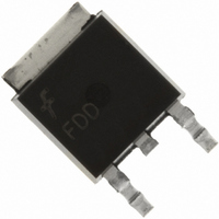
FDD6635 Fairchild Semiconductor, FDD6635 Datasheet - Page 7

FDD6635
Manufacturer Part Number
FDD6635
Description
MOSFET N-CH 35V 15A DPAK
Manufacturer
Fairchild Semiconductor
Series
PowerTrench®r
Datasheet
1.FDD6635.pdf
(8 pages)
Specifications of FDD6635
Fet Type
MOSFET N-Channel, Metal Oxide
Fet Feature
Logic Level Gate
Rds On (max) @ Id, Vgs
10 mOhm @ 15A, 10V
Drain To Source Voltage (vdss)
35V
Current - Continuous Drain (id) @ 25° C
15A
Vgs(th) (max) @ Id
3V @ 250µA
Gate Charge (qg) @ Vgs
36nC @ 10V
Input Capacitance (ciss) @ Vds
1400pF @ 20V
Power - Max
1.6W
Mounting Type
Surface Mount
Package / Case
DPak, TO-252 (2 leads+tab), SC-63
Configuration
Single
Transistor Polarity
N-Channel
Resistance Drain-source Rds (on)
0.01 Ohms
Drain-source Breakdown Voltage
35 V
Gate-source Breakdown Voltage
+/- 20 V
Continuous Drain Current
59 A
Power Dissipation
55 W
Maximum Operating Temperature
+ 150 C
Mounting Style
SMD/SMT
Minimum Operating Temperature
- 55 C
Lead Free Status / RoHS Status
Lead free / RoHS Compliant
Other names
FDD6635TR
Available stocks
Company
Part Number
Manufacturer
Quantity
Price
Company:
Part Number:
FDD6635
Manufacturer:
FAIRCHILD
Quantity:
35 000
Company:
Part Number:
FDD6635
Manufacturer:
FAIRCHILD
Quantity:
8 200
Test Circuits and Waveforms
FDD6635 Rev. C2(W)
Figure 14. Unclamped Inductive Load Test
+
+
-
-
10V
10V
R
R
Figure 18. Switching Time Test Circuit
GEN
GEN
V
V
Figure 16. Gate Charge Test Circuit
vary t
vary t
required peak I
required peak I
Drain Current Regulator
Drain Current Regulator
I
I
V
V
g(REF)
g(REF)
10μF
10μF
GS
GS
Same type as DUT
Same type as DUT
GS
GS
R
R
V
V
GEN
GEN
P
P
V
V
GS
GS
0V
0V
Pulse Width ≤ 1μs
Pulse Width ≤ 1μs
Duty Cycle ≤ 0.1%
Duty Cycle ≤ 0.1%
to obtain
to obtain
V
V
GS
GS
50kΩ
50kΩ
DS
DS
tp
tp
V
V
AS
AS
GS
GS
1μF
1μF
V
V
DS
DS
Circuit
I
I
AS
AS
0.01Ω
0.01Ω
DUT
DUT
L
L
DUT
DUT
DUT
DUT
R
R
L
L
+
+
-
-
V
V
DD
DD
+
+
-
-
+
+
-
-
V
V
V
V
DD
DD
DD
DD
V
V
V
V
V
V
Figure 15. Unclamped Inductive Waveforms
10V
10V
GS
GS
0V
0V
0V
0V
DS
DS
GS
GS
Figure 19. Switching Time Waveforms
10%
10%
Figure 17. Gate Charge Waveform
I
I
AS
AS
Q
Q
t
t
t
t
GS
GS
d(ON)
d(ON)
90%
90%
P
P
t
t
50%
50%
ON
ON
Charge, (nC)
Charge, (nC)
10%
10%
Q
Q
Pulse Width
Pulse Width
BV
BV
t
t
Q
Q
r
r
G
G
GD
GD
t
t
AV
AV
DSS
DSS
V
V
DS
DS
t
t
d(OFF)
d(OFF)
90%
90%
V
V
t
t
OFF
OFF
www.fairchildsemi.com
50%
50%
DD
DD
t
t
10%
10%
f
f
90%
90%


