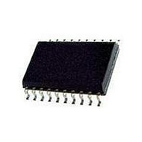
TDA8552TD NXP Semiconductors, TDA8552TD Datasheet - Page 5

TDA8552TD
Manufacturer Part Number
TDA8552TD
Description
Audio Amplifiers AUDIO PWR AMP BTL
Manufacturer
NXP Semiconductors
Datasheet
1.TDA8552TSN1118.pdf
(27 pages)
Specifications of TDA8552TD
Product
Class-AB
Output Power
1.4 W
Available Set Gain
30 dB
Thd Plus Noise
0.1 %
Operating Supply Voltage
5 V
Supply Current
14 mA
Maximum Power Dissipation
2200 mW
Maximum Operating Temperature
+ 85 C
Mounting Style
SMD/SMT
Audio Load Resistance
32 Ohms
Input Offset Voltage
5.5 V
Input Signal Type
Single
Minimum Operating Temperature
- 40 C
Output Signal Type
Differential, Single
Supply Type
Single
Supply Voltage (max)
5.5 V
Supply Voltage (min)
2.7 V
Output Type
2-Channel Stereo
Package / Case
SO-20
Lead Free Status / RoHS Status
Lead free / RoHS Compliant
Other names
TDA8552T/N1,512
NXP Semiconductors
PINNING
Note
1. For the SO20 (SOT163-1) package only: the ground
2002 Jan 04
GND1
OUT2+
V
HPS
MODE
UP/DOWN1
UP/DOWN2
V
OUT2−
GND2
GND3
OUT1+
V
GAINSEL
IN2
SVR
IN1
V
OUT1−
GND4
DD1
DD2
DD3
DD4
2 x 1.4 W BTL audio amplifiers with digital
volume control and headphone sensing
SYMBOL
pins 1, 10, 11 and 20 are mechanically connected to
the leadframe and electrically to the substrate of the
die. On the PCB the ground pins can be connected to
a copper area to decrease the thermal resistance.
PIN
10
12
13
14
15
16
17
18
19
20
11
1
2
3
4
5
6
7
8
9
(1)
ground 1, substrate/leadframe
positive loudspeaker terminal
output channel 2
supply voltage 1
digital input for headphone
sensing
digital trinary input for mode
selection (standby, mute and
operating)
digital trinary input for volume
control channel 1
digital trinary input for volume
control channel 2
supply voltage 2
negative loudspeaker terminal
output channel 2
ground 2, substrate/leadframe
ground 3, substrate/leadframe
positive loudspeaker terminal
output channel 1
supply voltage 3
digital input for gain selection
audio input channel 2
half supply voltage, decoupling
ripple rejection
audio input channel 1
supply voltage 4
negative loudspeaker terminal
output channel 1
ground 4, substrate/leadframe
DESCRIPTION
5
handbook, halfpage
UP/DOWN1
UP/DOWN2
OUT2
OUT2
MODE
GND1
GND2
V DD1
V DD2
HPS
Fig.2 Pin configuration.
TDA8552T; TDA8552TS
10
1
2
3
4
5
6
7
8
9
TDA8552T
MGM610
15
14
13
12
20
19
18
17
16
11
Product specification
GND4
OUT1
V DD4
IN1
SVR
IN2
GAINSEL
V DD3
OUT1
GND3


