UDA1345TSDB NXP Semiconductors, UDA1345TSDB Datasheet - Page 7
UDA1345TSDB
Manufacturer Part Number
UDA1345TSDB
Description
Audio CODECs AUDIO CODEC
Manufacturer
NXP Semiconductors
Datasheet
1.UDA1345TSN2112.pdf
(29 pages)
Specifications of UDA1345TSDB
Number Of Adc Inputs
2
Number Of Dac Outputs
2
Conversion Rate
100 KSPs
Interface Type
Serial (I2S), L3
Resolution
24 bit
Operating Supply Voltage
2.4 V to 3.6 V
Maximum Operating Temperature
+ 85 C
Mounting Style
SMD/SMT
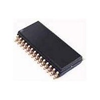
Package / Case
SSOP-28
Minimum Operating Temperature
- 40 C
Number Of Channels
2 ADC, 2 DAC
Snr
100 dB
Supply Current
10 mA
Lead Free Status / RoHS Status
Lead free / RoHS Compliant
Other names
UDA1345TS/N2,112


NXP Semiconductors
6
2002 May 28
V
V
VINL
V
VINR
V
V
MC1
MP1
V
V
SYSCLK
MP2
MP3
MP4
BCK
WS
DATAO
DATAI
MP5
MC2
V
V
VOUTR
V
VOUTL
V
V
SYMBOL
SSA(ADC)
DDA(ADC)
ref(A)
ADCN
ADCP
DDD
SSD
SSA(DAC)
DDA(DAC)
DDO
SSO
ref(D)
Economy audio CODEC
PINNING
PIN
10
12
13
14
15
16
17
18
19
20
21
22
23
24
25
26
27
28
11
1
2
3
4
5
6
7
8
9
analog ground pad
analog supply pad
analog input pad
analog pad
analog input pad
analog pad
analog pad
5 V tolerant digital input pad with internal pull-down pad
5 V tolerant slew rate controlled digital output pad
digital supply pad
digital ground pad
5 V tolerant digital Schmitt triggered input pad
3-level input pad
5 V tolerant digital Schmitt triggered input pad
3-level input pad
5 V tolerant digital Schmitt triggered input pad
5 V tolerant digital Schmitt triggered input pad
5 V tolerant slew rate controlled digital output pad
5 V tolerant digital Schmitt triggered input pad
5 V tolerant digital Schmitt triggered input pad
5 V tolerant digital input pad with internal pull-down pad
analog ground pad
analog supply pad
analog output pad
analog supply pad
analog output pad
analog ground pad
analog pad
TYPE
7
ADC analog ground
ADC analog supply voltage
ADC input left
ADC reference voltage
ADC input right
ADC negative reference voltage
ADC positive reference voltage
mode control 1 (pull-down)
multi purpose pin 1
digital supply voltage
digital ground
system clock 256, 384 or 512f
multi purpose pin 2
multi purpose pin 3
multi purpose pin 4
bit clock input
word select input
data output
data input
multi purpose pin 5 (pull down)
mode control 2 (pull-down)
DAC analog ground
DAC analog supply voltage
DAC output right
operational amplifier supply voltage
DAC output left
operational amplifier ground
DAC reference voltage
DESCRIPTION
UDA1345TS
Product specification
s
Related parts for UDA1345TSDB
Image
Part Number
Description
Manufacturer
Datasheet
Request
R

Part Number:
Description:
Economy audio CODEC
Manufacturer:
PHILIPS [NXP Semiconductors]
Datasheet:

Part Number:
Description:
NXP Semiconductors designed the LPC2420/2460 microcontroller around a 16-bit/32-bitARM7TDMI-S CPU core with real-time debug interfaces that include both JTAG andembedded trace
Manufacturer:
NXP Semiconductors
Datasheet:

Part Number:
Description:
NXP Semiconductors designed the LPC2458 microcontroller around a 16-bit/32-bitARM7TDMI-S CPU core with real-time debug interfaces that include both JTAG andembedded trace
Manufacturer:
NXP Semiconductors
Datasheet:
Part Number:
Description:
NXP Semiconductors designed the LPC2468 microcontroller around a 16-bit/32-bitARM7TDMI-S CPU core with real-time debug interfaces that include both JTAG andembedded trace
Manufacturer:
NXP Semiconductors
Datasheet:
Part Number:
Description:
NXP Semiconductors designed the LPC2470 microcontroller, powered by theARM7TDMI-S core, to be a highly integrated microcontroller for a wide range ofapplications that require advanced communications and high quality graphic displays
Manufacturer:
NXP Semiconductors
Datasheet:
Part Number:
Description:
NXP Semiconductors designed the LPC2478 microcontroller, powered by theARM7TDMI-S core, to be a highly integrated microcontroller for a wide range ofapplications that require advanced communications and high quality graphic displays
Manufacturer:
NXP Semiconductors
Datasheet:
Part Number:
Description:
The Philips Semiconductors XA (eXtended Architecture) family of 16-bit single-chip microcontrollers is powerful enough to easily handle the requirements of high performance embedded applications, yet inexpensive enough to compete in the market for hi
Manufacturer:
NXP Semiconductors
Datasheet:
Part Number:
Description:
The XA-S3 device is a member of Philips Semiconductors? XA(eXtended Architecture) family of high performance 16-bitsingle-chip microcontrollers
Manufacturer:
NXP Semiconductors
Datasheet:

Part Number:
Description:
The NXP BlueStreak LH75401/LH75411 family consists of two low-cost 16/32-bit System-on-Chip (SoC) devices
Manufacturer:
NXP Semiconductors
Datasheet:
Part Number:
Description:
The NXP LPC3130/3131 combine an 180 MHz ARM926EJ-S CPU core, high-speed USB2
Manufacturer:
NXP Semiconductors
Datasheet:
Part Number:
Description:
The NXP LPC3141 combine a 270 MHz ARM926EJ-S CPU core, High-speed USB 2
Manufacturer:
NXP Semiconductors
Part Number:
Description:
The NXP LPC3143 combine a 270 MHz ARM926EJ-S CPU core, High-speed USB 2
Manufacturer:
NXP Semiconductors

Part Number:
Description:
The NXP LPC3152 combines an 180 MHz ARM926EJ-S CPU core, High-speed USB 2
Manufacturer:
NXP Semiconductors
Part Number:
Description:
The NXP LPC3154 combines an 180 MHz ARM926EJ-S CPU core, High-speed USB 2
Manufacturer:
NXP Semiconductors