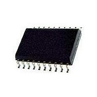
TDA8542AT/N1-T NXP Semiconductors, TDA8542AT/N1-T Datasheet - Page 8

TDA8542AT/N1-T
Manufacturer Part Number
TDA8542AT/N1-T
Description
Audio Amplifiers 2X1.5W BTL POWER AMP
Manufacturer
NXP Semiconductors
Datasheet
1.TDA8542ATN1512.pdf
(20 pages)
Specifications of TDA8542AT/N1-T
Product
Class-AB
Output Power
1.5 W
Available Set Gain
30 dB
Thd Plus Noise
0.15 %
Operating Supply Voltage
6 V
Maximum Power Dissipation
2200 mW
Maximum Operating Temperature
+ 85 C
Mounting Style
SMD/SMT
Audio Load Resistance
8 Ohms
Input Bias Current (max)
0.5 uA
Input Signal Type
Differential or Single
Minimum Operating Temperature
- 40 C
Output Signal Type
Differential, Single
Supply Type
Single
Supply Voltage (max)
18 V
Supply Voltage (min)
2.2 V
Output Type
2-Channel Stereo
Package / Case
SOT-163
Lead Free Status / RoHS Status
Lead free / RoHS Compliant
Other names
TDA8542AT/N1,518
Philips Semiconductors
TEST AND APPLICATION INFORMATION
Test conditions
Because the application can be either Bridge-Tied Load
(BTL) or Single-Ended (SE), the curves of each application
are shown separately.
The thermal resistance = 60 K/W; the maximum sine wave
power dissipation for T
For T
BTL application
T
f = 1 kHz, R
22 Hz to 22 kHz.
The BTL application diagram is illustrated in Fig.3.
The quiescent current has been measured without any
load impedance. The total harmonic distortion as a
function of frequency was measured with a low-pass filter
of 80 kHz. The value of capacitor C3 influences the
behaviour of the SVRR at low frequencies, increasing the
value of C3 increases the performance of the SVRR.
The figure of the mode select voltage (V
of the supply voltage shows three areas; operating, mute
and standby. It shows, that the DC-switching levels of the
mute and standby respectively depends on the supply
voltage level.
Thermal behaviour
The measured thermal resistance of the IC package is
highly dependent on the configuration and size of the
application board. Data may not be comparable between
different semiconductors manufacturers because the
application boards and test methods are not (yet)
standardized. Also, the thermal performance of packages
for a specific application may be different than presented
here, because the configuration of the application boards
(copper area) may be different.
Philips Semiconductors uses FR-4 type application boards
with 1 oz copper traces with solder coating.
The measurements have been carried out with vertical
placed boards.
1998 Mar 25
150 60
--------------------- -
amb
2
60
–
= 25 C if not specially mentioned, V
amb
1.5 W BTL audio amplifier
= 60 C the maximum total power dissipation is:
=
L
1.5 W
= 8 , G
v
amb
= 20 dB, audio band-pass
= 25 C is:
150 25
--------------------- -
ms
CC
60
) as a function
–
= 6 V,
=
2.1 W
8
Using a practical PCB layout with wider copper tracks and
some copper area to the IC pins and just under the IC
(see Fig.22), the thermal resistance from junction to
ambient can be reduced to approximately 56 K/W.
For T
at this PCB layout is:
For the application V
sine wave dissipation is 1.75 W.
SE application
T
f = 1 kHz, R
22 Hz to 22 kHz.
The SE application diagram is illustrated in Fig.14.
If the BTL/SE pin (pin 6) is connected to ground, the
positive outputs (pins 3 and 8) will be in mute condition
with a DC level of
(R
without output coupling capacitors; load between negative
output and one of the positive outputs (e.g. pin 3) as
common pin.
Increasing the value of electrolytic capacitor C3 will result
in a better channel separation. Because the positive output
is not designed for high output current (2
impedance ( 16 ), the SE application with output
capacitors connected to ground is advised. The capacitor
value of C4/C5 in combination with the load impedance
determines the low frequency behaviour. The THD as a
function of frequency was measured using a low-pass filter
of 80 kHz. The value of capacitor C3 influences the
behaviour of the SVRR at low frequencies, increasing the
value of C3 increases the performance of the SVRR.
General remark
The frequency characteristic can be adapted by
connecting a small capacitor across the feedback resistor.
To improve the immunity of HF radiation in radio circuit
applications, a small capacitor can be connected in
parallel with the feedback resistor (56 k ); this creates a
low-pass filter.
amb
L
amb(max)
= 25 C if not specially mentioned, V
25
L
the SE headphone application can be used
= 50 C the maximum total power dissipation
= 4 , G
1
2
CC
V
150 50
---------------------- -
CC
v
= 6 V and R
= 20 dB, audio band-pass
. When a headphone is used
56
–
=
1.79 W
L
TDA8542AT
= 8
Product specification
CC
the worst case
I
o
= 7.5 V,
) at low load


