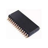
UDA1341TSDB NXP Semiconductors, UDA1341TSDB Datasheet - Page 11

UDA1341TSDB
Manufacturer Part Number
UDA1341TSDB
Description
Audio CODECs AUDIO CODEC MINIDISC
Manufacturer
NXP Semiconductors
Datasheet
1.UDA1341TSN1512.pdf
(34 pages)
Specifications of UDA1341TSDB
Number Of Adc Inputs
4
Number Of Dac Outputs
2
Conversion Rate
48 KSPs
Interface Type
Serial (I2S), L3
Resolution
20 bit
Operating Supply Voltage
2.4 V to 3.6 V
Maximum Operating Temperature
+ 85 C
Mounting Style
SMD/SMT
Package / Case
SSOP-28
Minimum Operating Temperature
- 20 C
Number Of Channels
2
Snr
100 dB
Supply Current
12.5 mA
Lead Free Status / RoHS Status
Lead free / RoHS Compliant
Other names
UDA1341TS/N1,512
NXP Semiconductors
7.18
The UDA1341TS has a microcontroller input mode. In the
microcontroller mode, all the digital sound processing
features and the system controlling features can be
controlled by the microcontroller.
The controllable features are:
• Reset
• System clock frequency
• Power control
• DAC gain switch
• ADC input gain switch
• ADC/DAC polarity control
• Double speed playback
• De-emphasis
• Volume
• Mode switch
• Bass boost
• Treble
• Mute
• MIC sensitivity control
• AGC control
• Input amplifier gain control
• Digital mixer control
• Peak detection position.
Via the L3-interface the peak level value of the signal in the
DAC path can be read out from the UDA1341TS to the
microcontroller.
The exchange of data and control information between the
microcontroller and the UDA1341TS is accomplished
through a serial hardware L3-interface comprising the
following pins:
• L3DATA: microcontroller interface data line
• L3MODE: microcontroller interface mode line
• L3CLOCK: microcontroller interface clock line.
Information transfer through the microcontroller bus is
organized in accordance with the so called ‘L3’ format, in
which two different modes of operation can be
distinguished: address mode and data transfer mode.
2002 May 16
Economy audio CODEC for MiniDisc (MD)
home stereo and portable applications
L3-interface
11
The address mode is required to select a device
communicating via the L3-bus and to define the
destination registers for the data transfer mode.
Data transfer can be in both directions: input to the
UDA1341TS to program its sound processing and system
controlling features and output from the UDA1341TS to
provide the peak level value.
7.19
The address mode is used to select a device for
subsequent data transfer and to define the destination
registers. The address mode is characterized by L3MODE
being LOW and a burst of 8 pulses on L3CLOCK,
accompanied by 8 data bits. The fundamental timing is
shown in Fig.5.
Data bits 7 to 2 represent a 6-bit device address, with bit 7
being the MSB and bit 2 the LSB. The address of the
UDA1341TS is 000101.
Data bits 0 to 1 indicate the type of the subsequent data
transfer as shown in Table 4.
In the event that the UDA1341TS receives a different
address, it will deselect its microcontroller interface logic.
7.20
The selection activated in the address mode remains
active during subsequent data transfers, until the
UDA1341TS receives a new address command.
The fundamental timing of data transfers is essentially the
same as the timing in the address mode and is given in
Fig.6.
Note that ‘L3DATA write’ denotes data transfer from the
microcontroller to the UDA1341TS and ‘L3DATA peak
read’ denotes data transfer in the opposite direction.
The maximum input clock and data rate is 64f
All transfers are byte-wise, i.e. they are based on groups
of 8 bits. Data will be stored in the UDA1341TS after the
eighth bit of a byte has been received.
A multibyte transfer is illustrated in Fig.7.
Address mode
Data transfer mode
UDA1341TS
Product specification
s
.


