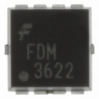
FDM3622 Fairchild Semiconductor, FDM3622 Datasheet - Page 2

FDM3622
Manufacturer Part Number
FDM3622
Description
MOSFET N-CH 100V 4.4A POWER33
Manufacturer
Fairchild Semiconductor
Series
PowerTrench®r
Datasheet
1.FDM3622.pdf
(7 pages)
Specifications of FDM3622
Fet Type
MOSFET N-Channel, Metal Oxide
Fet Feature
Logic Level Gate
Rds On (max) @ Id, Vgs
60 mOhm @ 4.4A, 10V
Drain To Source Voltage (vdss)
100V
Current - Continuous Drain (id) @ 25° C
4.4A
Vgs(th) (max) @ Id
4V @ 250µA
Gate Charge (qg) @ Vgs
17nC @ 10V
Input Capacitance (ciss) @ Vds
1090pF @ 25V
Power - Max
900mW
Mounting Type
Surface Mount
Package / Case
8-MLP, Power33
Configuration
Single Quad Drain Triple Source
Transistor Polarity
N-Channel
Resistance Drain-source Rds (on)
0.06 Ohm @ 10 V
Drain-source Breakdown Voltage
100 V
Gate-source Breakdown Voltage
+/- 20 V
Continuous Drain Current
4.4 A
Power Dissipation
2100 mW
Maximum Operating Temperature
+ 150 C
Mounting Style
SMD/SMT
Minimum Operating Temperature
- 55 C
Lead Free Status / RoHS Status
Lead free / RoHS Compliant
Other names
FDM3622
FDM3622TR
FDM3622TR
Available stocks
Company
Part Number
Manufacturer
Quantity
Price
Company:
Part Number:
FDM3622
Manufacturer:
AIT
Quantity:
6 000
Part Number:
FDM3622
Manufacturer:
FAIRCHILD/ن»™ç«¥
Quantity:
20 000
Part Number:
FDM3622NZ
Manufacturer:
FAIRCHILD/ن»™ç«¥
Quantity:
20 000
FDM3622 Rev.B
Electrical Characteristics
Off Characteristics
On Characteristics
Dynamic Characteristics
Switching Characteristics
Drain-Source Diode Characteristics
Notes:
1: R
2: Pulse Test: Pulse Width < 300μs, Duty cycle < 2.0%.
BV
I
I
V
r
C
C
C
Rg
t
t
t
t
Q
Q
Q
V
t
Q
DSS
GSS
d(on)
r
d(off)
f
rr
DS(on)
(a)R
(b)R
GS(th)
SD
iss
oss
rss
g
gs
gd
rr
user's board design.
Symbol
DSS
θJA
θJA
θJA
is determined with the device mounted on a 1 in
= 60°C/W when mounted on a 1 in
= 135°C/W when mounted on a minimum pad of 2 oz copper.
Drain to Source Breakdown Voltage
Zero Gate Voltage Drain Current
Gate to Source Leakage Current
Gate to Source Threshold Voltage
Static Drain to Source On Resistance
Input Capacitance
Output Capacitance
Reverse Transfer Capacitance
Gate Resistance
Turn-On Delay Time
Rise Time
Turn-Off Delay Time
Fall Time
Total Gate Charge
Gate to Source Gate Charge
Gate to Drain “Miller” Charge
Source to Drain Diode Forward Voltage
Reverse Recovery Time
Reverse Recovery Charge
Parameter
2
pad of 2 oz copper, 1.5’x1.5’x0.062’ thick PCB.
a. 60°C/W when mounted on
a 1 in
T
2
2
J
pad of 2 oz copper
oz copper pad on a 1.5 x 1.5 in. board of FR-4 material. R
= 25°C unless otherwise noted
V
V
V
V
V
V
V
V
I
V
V
V
f = 1MHz
V
V
V
I
I
D
F
D
GS
GS
GS
GS
DD
GS
GS
DD
DS
GS
GS
GS
DS
DS
= 4.4A, di/dt = 100A/μs
= 250μA, V
= 4.4A
= 10V
= V
= 10V, I
= 6.0V, I
= 10V, I
= 50V, I
= 10V, R
= 50V
= 80V, V
= 25V, V
= 15mV, f = 1MHz
= 0V, I
= 0V, I
= ±20V, V
2
DS
Test Conditions
, I
S
S
D
D
D
D
= 4.4A
= 2.2A
D
GEN
GS
GS
GS
= 4.4A
= 4.4A
= 4.4A , T
DS
= 250μA
= 3.8A
= 0V
= 0V,
= 0V
= 0V
= 24Ω
T
J
= 100°C
J
= 150°C
θJC
is guaranteed by design while R
b. 135°C/W when mounted on a
minimum pad of 2 oz copper
Min
100
2
3.6
3.4
Typ
25
35
26
13
820
125
11
3.1
44
56
92
35
θJA
1.25
±100
Max
108
1090
1.0
250
120
20
40
56
42
17
56
170
is determined by the
www.fairchildsemi.com
60
80
55
1
4
Units
mΩ
nC
nC
nC
nC
μA
nA
ns
ns
ns
ns
ns
pF
pF
pF
V
V
V
V
Ω


