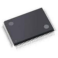
ISPPAC-CLK5520V-01TN100C Lattice, ISPPAC-CLK5520V-01TN100C Datasheet - Page 19

ISPPAC-CLK5520V-01TN100C
Manufacturer Part Number
ISPPAC-CLK5520V-01TN100C
Description
Clock Drivers & Distribution PROGRAMMABLE CLOCK GENERATOR
Manufacturer
Lattice
Datasheet
1.PAC-SYSTEMCLK5520.pdf
(48 pages)
Specifications of ISPPAC-CLK5520V-01TN100C
Minimum Operating Temperature
0 C
Mounting Style
SMD/SMT
Maximum Operating Temperature
70 C
Package / Case
TQFP-100
Lead Free Status / RoHS Status
Lead free / RoHS Compliant
Available stocks
Company
Part Number
Manufacturer
Quantity
Price
Company:
Part Number:
ISPPAC-CLK5520V-01TN100C
Manufacturer:
Lattice Semiconductor Corporation
Quantity:
10 000
Lattice Semiconductor
Figure 13 shows the relative timing for a V-divider as a function of its 32 possible divisor settings (2-64) as the PLL
locks. If two V-dividers are configured with the same divisor, their outputs will be synchronized. If these two V-divid-
ers are fed to separate outputs, and the skew settings for these two outputs are identical, then the corresponding
rising and falling edges for the two outputs will occur simultaneously.
Figure 13. ispClock5500 Output Divider Timing Relationships Among Various Divisors
If two V-dividers are configured with different divisors, however, their outputs may not necessarily have aligned
edges, even in cases where one divisor is an integer multiple of the other (e.g. 6 and 12). In cases where the divi-
sor is set to either 2 or a multiple of 4, the output duty cycle will be 50% (top set of waveforms in Figure 13), and the
rising edges (or falling edges) of outputs driven from different divisors may be aligned by inverting one or more of
the outputs as shown in Figure 14.
LOCK
/32
/38
/42
/46
/54
/58
/12
/16
/20
/24
/28
/36
/40
/44
/48
/52
/56
/60
/64
/10
/14
/18
/22
/26
/30
/34
/50
/62
/2
/4
/8
/6
0
10
20
19
VCO Clock Periods
30
ispClock5500 Family Data Sheet
40
50
60


