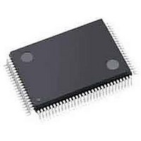
ISPPAC-CLK5520V-01TN100C Lattice, ISPPAC-CLK5520V-01TN100C Datasheet - Page 28

ISPPAC-CLK5520V-01TN100C
Manufacturer Part Number
ISPPAC-CLK5520V-01TN100C
Description
Clock Drivers & Distribution PROGRAMMABLE CLOCK GENERATOR
Manufacturer
Lattice
Datasheet
1.PAC-SYSTEMCLK5520.pdf
(48 pages)
Specifications of ISPPAC-CLK5520V-01TN100C
Minimum Operating Temperature
0 C
Mounting Style
SMD/SMT
Maximum Operating Temperature
70 C
Package / Case
TQFP-100
Lead Free Status / RoHS Status
Lead free / RoHS Compliant
Available stocks
Company
Part Number
Manufacturer
Quantity
Price
Company:
Part Number:
ISPPAC-CLK5520V-01TN100C
Manufacturer:
Lattice Semiconductor Corporation
Quantity:
10 000
Lattice Semiconductor
Figure 26. Maximum Ambient Temperature vs. Number of Active Output Banks
Figure 26b shows another derating curve, derived under the assumption that the output frequency is 100MHz. For
many applications, 100MHz outputs will be a more realistic scenario. Comparing the maximum temperature limits
of Figure 26b with Figure 26a, one can see that significantly higher operating temperatures are possible in LVC-
MOS 3.3V output mode with more outputs at 100MHz than at 320MHz.
The examples above described examples using LVCMOS 3.3V logic, which represents the maximum power dissi-
pation case at higher frequencies. For optimal operation at very high frequencies (> 150 MHz) LVDS will often be
the best choice from a signal integrity standpoint. For LVDS-configured outputs, the maximum ICCO current con-
sumption per bank is low enough that both the ispClock5510 and ispClock5520 can operate all outputs at maxi-
mum frequency over their complete rated temperature range, as shown in Figure 26c.
Note that because of variations in circuit board mounting, construction, and layout, as well as convective and forced
airflow present in a given design, actual die operating temperature is subject to considerable variation from that
which may be theoretically predicted from package characteristics and device power dissipation.
Output Enable Controls
The ispClock5500 family provides the user with several options for enabling and disabling output pins, as well as
suspending the output clock. In addition to providing the user with the ability to reduce the device’s power con-
sumption by turning off unused drivers, these features can also be used for functional testing purposes. The follow-
ing inputs pins are used for output enable functions:
90
80
70
60
50
40
90
80
70
60
50
40
0
(Outputs LVCMOS 3.3V, f
0
(Outputs LVDS, f
Temperature Derating Curves
Temperature Derating Curves
2
2
# Active Output Banks
# Active Output Banks
4
4
(c)
(a)
OUT
6
6
=320 MHz)
OUT
=320 MHz)
8
8
10
10
28
90
80
70
60
50
40
0
(Outputs LVCMOS 3.3V, f
Temperature Derating Curves
5520 Commercial
5520 Industrial
5510 Commericial
5510 Industrial
2
ispClock5500 Family Data Sheet
# Active Output Banks
4
(b)
6
OUT
=100 MHz)
8
10


