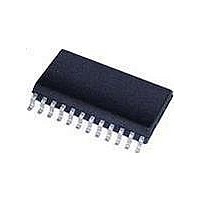
PCK351D-T NXP Semiconductors, PCK351D-T Datasheet - Page 5

PCK351D-T
Manufacturer Part Number
PCK351D-T
Description
Clock Buffer 1:10 CLK DISTR DEV 3-ST OUTPUT
Manufacturer
NXP Semiconductors
Datasheet
1.PCK351D112.pdf
(18 pages)
Specifications of PCK351D-T
Number Of Outputs
10
Propagation Delay (max)
4.1 ns
Supply Voltage (max)
3.6 V
Supply Voltage (min)
3 V
Maximum Power Dissipation
650 mW
Maximum Operating Temperature
+ 85 C
Minimum Operating Temperature
- 40 C
Mounting Style
SMD/SMT
Package / Case
SO-24
Lead Free Status / RoHS Status
Lead free / RoHS Compliant
Other names
PCK351D,118
Philips Semiconductors
7. Functional description
PCK351_2
Product data sheet
7.1 Function table
7.2 Logic symbol
Refer to
Table 4:
H = HIGH voltage level; L = LOW voltage level; Z = high-impedance OFF-state
Fig 4. Logic symbol
Figure 1 “Logic diagram of
A
H
H
L
L
Function table
Inputs
Rev. 02 — 16 December 2005
OE
H
H
L
L
OE
A
1 : 10 clock distribution device with 3-state outputs
5
6
PCK351”.
EN
002aaa283
23
21
19
18
16
14
11
9
4
2
Y1
Y2
Y3
Y4
Y5
Y6
Y7
Y8
Y9
Y10
© Koninklijke Philips Electronics N.V. 2005. All rights reserved.
Outputs
Yn
H
Z
Z
L
PCK351
5 of 18


