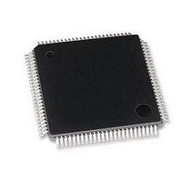
LAN91C96-MS SMSC, LAN91C96-MS Datasheet - Page 42

LAN91C96-MS
Manufacturer Part Number
LAN91C96-MS
Description
Ethernet ICs Non-PCI 10 Mbps Ethernet MAC
Manufacturer
SMSC
Type
Single Chip MAC and PHY Controllerr
Datasheet
1.LAN91C96-MU.pdf
(125 pages)
Specifications of LAN91C96-MS
Ethernet Connection Type
10 Base-T, 100 Base-TX
Minimum Operating Temperature
0 C
Mounting Style
SMD/SMT
Product
Ethernet Controllers
Number Of Transceivers
1
Standard Supported
802.3, 802.3u
Data Rate
10 Mbps, 100 Mbps
Supply Voltage (max)
5 V
Supply Voltage (min)
0 V
Supply Current (max)
95 mA
Maximum Operating Temperature
+ 70 C
Package / Case
TQFP-100
Lead Free Status / RoHS Status
Lead free / RoHS Compliant
Available stocks
Company
Part Number
Manufacturer
Quantity
Price
Company:
Part Number:
LAN91C96-MS
Manufacturer:
Silex
Quantity:
115
Company:
Part Number:
LAN91C96-MS
Manufacturer:
Standard
Quantity:
1 578
Part Number:
LAN91C96-MS
Manufacturer:
SMSC
Quantity:
20 000
Chapter 7 Registers Map in I/O Space
7.1
7.2
Revision 1.0 (10-24-08)
I/O Space Access
The address is determined by the Ethernet I/O Base Registers. The Ethernet I/O space can be configured
as an 8 or 16 bit I/O space, and is similar to the LAN91C94, LAN91C92, etc. I/O space mapping. To limit
the I/O space requirements to 16 locations, the registers are Split into 4 banks in LOCAL BUS mode and 5
banks in PCMCIA mode. The last word of the I/O area is shared by all banks and can be used to change
the bank in use. Banks 0 through 3 functionally correspond to the LAN91C94 banks, while Bank 4 allows
access to the PCMCIA registers in LOCAL BUS mode.
Registers are described using the following convention:
OFFSET - Defines the address offset within the IOBASE where the register can be accessed at, provided
the bank select has the appropriate value. The offset specifies the address of the even byte (bits 0-7) or
the address of the complete word. The odd byte can be accessed using address (offset + 1).
Some registers (e.g. the Interrupt Ack. or the Interrupt Mask) are functionally described as two eight bit
registers. In such case, the offset of each one is independently specified.
Regardless of the functional description, when the LAN91C96 is in 16 bit mode, all registers can be
accessed as words or bytes.
RST Val - The default bit values upon hard reset are highlighted below each register.
I/O Space Registers Description
(Bank 4 Registers are described under PCMCIA Configuration Registers and will not be described again).
BIT 15
BIT 7
RST
RST
Val
Val
OFFSET
E
BIT14
BIT 6
RST
RST
Val
Val
BIT 13
BANK SELECT
BIT 5
RST
RST
Val
Val
REGISTER
DATASHEET
NAME
BIT 12
BIT 4
RST
RST
Val
Val
Page 42
BIT 11
BIT 3
Non-PCI Single-Chip Full Duplex Ethernet Controller with Magic Packet
RST
RST
READ/WRITE
Val
Val
TYPE
BIT 10
BIT 2
RST
RST
Val
Val
BIT 1
BIT9
RST
RST
Val
Val
SYMBOL
BSR
BIT 0
BIT8
RST
RST
Val
Val
SMSC LAN91C96 5v&3v
Datasheet


