IRFR9020TRPBF Vishay, IRFR9020TRPBF Datasheet
IRFR9020TRPBF
Specifications of IRFR9020TRPBF
Available stocks


Related parts for IRFR9020TRPBF


IRFR9020TRPBF Summary of contents
Page 1
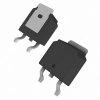
... IRFU9020, SiHFU9020 of the device is called the IPAK (TO-251). They are well suited for applications where limited heat dissipation is required such as, computers and peripherals, telecommunication equipment, dc-to-dc converters, and a wide range of consumer products. DPAK (TO-252) SiHFR9020TR-GE3 a IRFR9020TRPbF a SiHFR9020T-E3 a IRFR9020TR a SiHFR9020T = 25 °C, unless otherwise noted ° ...
Page 2
... IRFR9020, IRFU9020, SiHFR9020, SiHFU9020 Vishay Siliconix ABSOLUTE MAXIMUM RATINGS T PARAMETER b Single Pulse Avalanche Energy a Repetitive Avalanche Current a Repetitive Avalanche Energy Maximum Power Dissipation c Peak Diode Recovery dV/dt Operating Junction and Storage Temperature Range Soldering Recommendations (Peak Temperature) Notes a. Repetitive rating; pulse width limited by maximum junction temperature (see fig. 14). ...
Page 3
... SYMBOL TEST CONDITIONS MOSFET symbol I S showing the integral reverse junction diode ° 9 ° 9,7 A, dI/dt = 100 A/μ Intrinsic turn-on time is negligible (turn-on is dominated Vishay Siliconix MIN. TYP. MAX 9 6 110 280 b 0.17 0.34 0.85 and L S Fig Typical Saturation Characteristics Fig ...
Page 4
... IRFR9020, IRFU9020, SiHFR9020, SiHFU9020 Vishay Siliconix Fig Typical Transconductance vs. Drain Current Fig Typical Source-Drain Diode Forward Voltage www.vishay.com 4 Fig Breakdown Voltage vs. Temperature Fig Normalized On-Resistance vs. Temperature Document Number: 90350 S10-1135-Rev. C, 10-May-10 ...
Page 5
... Fig Typical Capacitance vs. Drain-to-Source Voltage Fig Typical Gate Charge vs. Gate-to-Source Voltage Document Number: 90350 S10-1135-Rev. C, 10-May-10 IRFR9020, IRFU9020, SiHFR9020, SiHFU9020 Fig Typical On-Resistance vs. Drain Current Fig Maximum Drain Current vs. Case Temperature Vishay Siliconix www.vishay.com 5 ...
Page 6
... IRFR9020, IRFU9020, SiHFR9020, SiHFU9020 Vishay Siliconix Fig. 13a - Maximum Avalanche vs. Starting Junction Temperature Fig Maximum Effective Transient Thermal Impedance, Junction-to-Case vs. Pulse Duration www.vishay.com 6 Fig. 13b - Unclamped Inductive Test Circuit Fig. 13c - Unclamped Inductive Waveforms Document Number: 90350 S10-1135-Rev. C, 10-May-10 ...
Page 7
... Fig. 15a - Switching Time Waveforms Charge Fig. 16a - Basic Gate Charge Waveform Document Number: 90350 S10-1135-Rev. C, 10-May-10 IRFR9020, IRFU9020, SiHFR9020, SiHFU9020 t t d(off) f Vishay Siliconix Fig. 15b - Switching Time Test Circuit Fig. 16b - Gate Charge Test Circuit www.vishay.com 7 ...
Page 8
... Note Vishay Siliconix maintains worldwide manufacturing capability. Products may be manufactured at one of several qualified locations. Reliability data for Silicon Technology and Package Reliability represent a composite of all qualified locations. For related documents such as package/tape drawings, part marking, and reliability data, see www.vishay.com/ppg?90350. www.vishay.com ...
Page 9
... Vishay product could result in personal injury or death. Customers using or selling Vishay products not expressly indicated for use in such applications their own risk and agree to fully indemnify and hold Vishay and its distributors harmless from and against any and all claims, liabilities, expenses and damages arising or resulting in connection with such use or sale, including attorneys fees, even if such claim alleges that Vishay or its distributor was negligent regarding the design or manufacture of the part ...