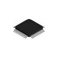
HV461FG Supertex, HV461FG Datasheet - Page 12

HV461FG
Manufacturer Part Number
HV461FG
Description
Telephone Ringers Controller IC
Manufacturer
Supertex
Datasheet
1.HV461FG-G.pdf
(14 pages)
Specifications of HV461FG
Function
Telecom Ringer
Mounting Style
SMD/SMT
Operating Supply Voltage
7 V
Product
Telecom Ringer
Package / Case
TQFP-48
Frequency
12 Hz, 16.66 Hz, 20 Hz
Maximum Operating Temperature
+ 85 C
Minimum Operating Temperature
- 40 C
Primary Target Application
Generator Circuit
Lead Free Status / RoHS Status
Lead free / RoHS Compliant
Available stocks
Company
Part Number
Manufacturer
Quantity
Price
Company:
Part Number:
HV461FG
Manufacturer:
ALPHA
Quantity:
3 000
Pin Description (cont.)
Pin
13
14
15
16
17
18
19
20
21
22
23
24
25
26
27
28
29
30
SYNCMODE
ENABLE
FREQ0
FREQ1
FREQ2
FAULT
DGND
SYNC
AMP0
AMP1
OFF0
OFF1
Name
TDLY
SW4
SW3
SW2
TDB
LE
Description
With SYNCMODE low, ringer output ceases the instant ENABLE goes low. When high, ringer
output ceases at the next ring signal phase crossing (0º/180º) after ENABLE goes low.
Outputs a pulse indicating sine reference 0º and 180º phase crossing (not to be confused with
zero–voltage crossing). The rising edge precedes phase crossing by a user–adjustable time
period (see TSYNC pin 44). Falling edge coincides with sine reference phase crossing. SYNC is
digitally derived, therefore phase shifts caused by the external filter capacitor at SINEREF will not
be reflected at the SYNC output.
Indicates abnormal operating conditions of output overcurrent, supply undervoltage (VDD &
VGD), or PWM overrange (duty cycle limit – see VDCL, pin 3). Together, these 3 conditions catch
most any problem. When an overcurrent or overrange condition exists for more than 8% of the
time, this output becomes active. It is cleared when the problem occurs less than 2% of the time.
Undervoltage conditions immediately activate the FAULT output. It is active low and open drain to
allow wire-ORing. See CFAULT (pin 15) for additional information.
Ringer output enable. Active high. When enabled, the ring signal always starts immediately at 0
degrees. If AMP≠00, SW1 and SW2 are held off when ENABLE=0 but SW3 and SW4 continue
switching. If AMP=00, SW3 and SW4 are held off as well. When disabled, the error amplifier
is set at unity gain to prevent saturation, reducing turn-on glitches when re-enabled. See
SYNCMODE (pin 13) for additional information.
Sets ring DC offset. Offset changes are effected at the next phase crossing (0º/180º) of the ring
signal. Except for 00, offsets are set by the voltages at DCREF1–3. (OFF0 is LSB) Offset = ½ x
Gain x (V
Sets ring amplitude. Amplitude changes are effected at the next phase crossing (0º/180º) of the
ring signal. Amplitudes, as a percentage of full scale, are: (AMP0 is LSB)
Full scale amplitude = 0.707V
Sets ring frequency. Frequency changes are effected at the next phase crossing (0º/180º) of the
ring signal.
Frequencies when using a 19.6608MHz crystal are: (FREQ0 is LSB)
Latch enable. The latch gates control inputs FREQ0–2, AMP0–1, OFF0–1, and ENABLE. When
LE is high, latch outputs follow inputs. On a low–going transition, outputs are latched.
An RC network on this pin sets the primary to secondary switch delay. This prevents the
secondary–side switches (SW3&4) from turning on prematurely. t
An RC network on this pin sets the deadband (break–before–make time) on the primary–side
switches (SW1&2). Deadband prevents both switches from conducting simultaneously.
Digital ground. Connect to AGND and PGND close to the IC.
Secondary–side switch driver output.
Secondary–side switch driver output.
Primary–side N-channel switch driver output.
t
DB
= 0.48RC
DCREFx
00 = 0V
000 = 16.7Hz
100 = 33.3Hz
●
00 = 0%
1235 Bordeaux Drive, Sunnyvale, CA 94089
- V
REF1
)
RMS
01 = DCREF1
001 = 20Hz
101 = 40Hz
01 = 50%
x Gain
12
●
Tel: 408-222-8888
010 = 25Hz
110 = 50Hz
10 = DCREF2
10 = 75%
DLY
●
= 0.48RC
www.supertex.com
11 = DCREF3
011 = 30Hz
111 = 60Hz
11 = 100%
HV461


