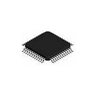
HV461FG Supertex, HV461FG Datasheet - Page 13

HV461FG
Manufacturer Part Number
HV461FG
Description
Telephone Ringers Controller IC
Manufacturer
Supertex
Datasheet
1.HV461FG-G.pdf
(14 pages)
Specifications of HV461FG
Function
Telecom Ringer
Mounting Style
SMD/SMT
Operating Supply Voltage
7 V
Product
Telecom Ringer
Package / Case
TQFP-48
Frequency
12 Hz, 16.66 Hz, 20 Hz
Maximum Operating Temperature
+ 85 C
Minimum Operating Temperature
- 40 C
Primary Target Application
Generator Circuit
Lead Free Status / RoHS Status
Lead free / RoHS Compliant
Available stocks
Company
Part Number
Manufacturer
Quantity
Price
Company:
Part Number:
HV461FG
Manufacturer:
ALPHA
Quantity:
3 000
Pin
31
32
33
34
35
36
37
38
39
40
41
42
43
44
45
46
47
48
DIFFAMPO
DIFFAMP+
DIFFAMP-
CLCOMP
SINEREF
COMP2
COMP1
DCREF1
DCREF2
PGND
DVDD
AGND
Name
VDCL
SW1
VGD
VDR
CL+
CL-
Description
Primary–side P-channel switch driver output.
Power ground. Connect to AGND and DGND close to the IC.
Supply for the SW1–4 drivers. An external boost converter controlled by VDR provides 9.6V for
driving the power stage MOSFETs. An undervoltage condition on this supply pin disables ringer
output and activates the FAULT output.
Gate drive for the external boost converter circuit. Outputs a fixed 50% duty cycle at the ringer
PWM frequency (see ROSC, pin 9). Output voltage regulation is via burp-mode operation. This
output is boostrapped to VGD, thus during startup VDR amplitude is VDD and after startup is
VGD. (See VGD, pin 33)
Supply for the digital section. 3.0V to 3.6V input. Undervoltage disables ringer output. Must be
from the same source as AVDD. Bypass with a 100nF capacitor to ground as close as possible
to the IC. An undervoltage condition on this supply pin disables ringer output and activates the
FAULT output.
Current limit amplifier non-inverting input.
Current limit amplifier inverting input.
Current limit compensation. An RC network connected between this pin and CL- establishes
current limit reaction time and stability.
Differential amplifier non-inverting input.
Differential amplifier inverting input.
Differential amplifier output.
Error amplifier compensation. An RC network connected between these pins establishes loop
stability.
COMP1 is the error amp inverting input. COMP2 is the error amp output.
Sine wave reference. Amplitude is 2V
external 33nF capacitor from this pin to ground should be employed to remove high frequency
synthesizer ripple. Synthesizer ripple is at a frequency of 2
Analog ground. Connect to AGND and DGND close to the IC.
Voltage applied to this pin sets the min/max duty cycle limits. If the PWM controller hits these limits, clipping
of the ringer output will occur and the FAULT output will be activated. D
In conjunction with the OFFx control inputs, voltages applied to these inputs set the output DC offset. Output
offset is the selected DCREFx voltage multiplied by gain. See also OFF0 & OFF1 (pins 17 & 18)
●
1235 Bordeaux Drive, Sunnyvale, CA 94089
13
P-P
nominal. Output impedance is approximately 16kΩ. An
The differential amplifier sets gain, establishing output
amplitude and DC offset in conjunction with AMPx and
OFFx.
Gain = R
see schematic)
●
FB2
Tel: 408-222-8888
/R
FB1
(R
15
· f
FB3
RING
= R
MIN
●
= 0.4V
FB1
www.supertex.com
and R
DCL
FB4
D
MAX
= R
= 1 - 0.4V
FB2
,
HV461
DCL


