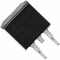
FDB8441 Fairchild Semiconductor, FDB8441 Datasheet - Page 6

FDB8441
Manufacturer Part Number
FDB8441
Description
MOSFET N-CH 40V 80A D2PAK
Manufacturer
Fairchild Semiconductor
Series
PowerTrench®r
Datasheet
1.FDB8441.pdf
(7 pages)
Specifications of FDB8441
Fet Type
MOSFET N-Channel, Metal Oxide
Fet Feature
Logic Level Gate
Rds On (max) @ Id, Vgs
2.5 mOhm @ 80A, 10V
Drain To Source Voltage (vdss)
40V
Current - Continuous Drain (id) @ 25° C
80A
Vgs(th) (max) @ Id
4V @ 250µA
Gate Charge (qg) @ Vgs
280nC @ 10V
Input Capacitance (ciss) @ Vds
15000pF @ 25V
Power - Max
300W
Mounting Type
Surface Mount
Package / Case
D²Pak, TO-263 (2 leads + tab)
Configuration
Single
Transistor Polarity
N-Channel
Resistance Drain-source Rds (on)
0.0019 Ohms @ 10 V
Drain-source Breakdown Voltage
40 V
Gate-source Breakdown Voltage
+/- 20 V
Continuous Drain Current
80 A
Power Dissipation
300 W
Maximum Operating Temperature
+ 175 C
Mounting Style
SMD/SMT
Minimum Operating Temperature
- 55 C
Lead Free Status / RoHS Status
Lead free / RoHS Compliant
Other names
FDB8441TR
Available stocks
Company
Part Number
Manufacturer
Quantity
Price
Company:
Part Number:
FDB8441
Manufacturer:
FAIRCHILD
Quantity:
12 500
FDB8441 Rev.A
Typical Characteristics
Figure 11.
Figure 13.
40000
10000
1000
1.2
1.0
0.8
0.6
0.4
100
-80
0.1
f = 1MHz
V
Normalized Gate Threshold Voltage vs
GS
-40
V
Junction Temperature
= 0V
Capacitance vs Drain to Source
DS
T
J
, DRAIN TO SOURCE VOLTAGE
, JUNCTION TEMPERATURE
0
Voltage
1
40
C
80
rss
120
10
(
V
I
C
D
o
C
GS
oss
C
iss
=
160
)
(
250
=
V
)
V
DS
µ
A
200
50
6
Figure 14.
Breakdown Voltage vs Junction Temperature
10
1.15
1.10
1.05
1.00
0.95
0.90
Figure 12. Normalized Drain to Source
8
6
4
2
0
0
-80
I
D
= 80A
I
D
Gate Charge vs Gate to Source Voltage
= 250
-40
50
T
µ
J
V
A
, JUNCTION TEMPERATURE
DD
Q
= 20V
g
0
, GATE CHARGE(nC)
100
V
40
DD
= 15V
150
80
www.fairchildsemi.com
120
V
200
DD
(
= 25V
o
C
160
)
250
200


