IRFI740GLCPBF Vishay, IRFI740GLCPBF Datasheet - Page 5
IRFI740GLCPBF
Manufacturer Part Number
IRFI740GLCPBF
Description
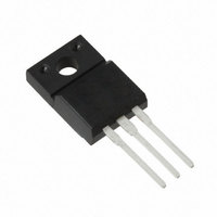
MOSFET N-CH 400V 5.7A TO220FP
Manufacturer
Vishay
Datasheet
1.IRFI740GLCPBF.pdf
(8 pages)
Specifications of IRFI740GLCPBF
Transistor Polarity
N-Channel
Fet Type
MOSFET N-Channel, Metal Oxide
Fet Feature
Standard
Rds On (max) @ Id, Vgs
550 mOhm @ 3.4A, 10V
Drain To Source Voltage (vdss)
400V
Current - Continuous Drain (id) @ 25° C
5.7A
Vgs(th) (max) @ Id
4V @ 250µA
Gate Charge (qg) @ Vgs
39nC @ 10V
Input Capacitance (ciss) @ Vds
1100pF @ 25V
Power - Max
40W
Mounting Type
Through Hole
Package / Case
TO-220-3 Full Pack (Straight Leads, Isolated), ITO-220AB
Minimum Operating Temperature
- 55 C
Configuration
Single
Resistance Drain-source Rds (on)
0.55 Ohm @ 10 V
Forward Transconductance Gfs (max / Min)
3 S
Drain-source Breakdown Voltage
400 V
Gate-source Breakdown Voltage
+/- 30 V
Continuous Drain Current
5.7 A
Power Dissipation
40000 mW
Maximum Operating Temperature
+ 150 C
Mounting Style
Through Hole
Continuous Drain Current Id
5.7A
Drain Source Voltage Vds
400V
On Resistance Rds(on)
550mohm
Rds(on) Test Voltage Vgs
10V
Threshold Voltage Vgs Typ
4V
Lead Free Status / RoHS Status
Lead free / RoHS Compliant
Lead Free Status / RoHS Status
Lead free / RoHS Compliant, Lead free / RoHS Compliant
Other names
*IRFI740GLCPBF


Document Number: 91155
S09-0012-Rev. A, 19-Jan-09
Vary t
required I
Fig. 9 - Maximum Drain Current vs. Case Temperature
p
Fig. 12a - Unclamped Inductive Test Circuit
to obtain
AS
R
10 V
G
V
DS
t
p
Fig. 11 - Maximum Effective Transient Thermal Impedance, Junction-to-Case
I
AS
D.U.T.
0.01 Ω
L
+
-
V
DD
Fig. 12b - Unclamped Inductive Waveforms
IRFI740GLC, SiHFI740GLC
90 %
10 %
V
V
V
I
DS
GS
AS
Fig. 10a - Switching Time Test Circuit
Fig. 10b - Switching Time Waveforms
DS
R
Pulse width ≤ 1 µs
Duty factor ≤ 0.1 %
G
10 V
t
V
d(on)
GS
V
DS
t
r
t
p
D.U.T.
Vishay Siliconix
R
D
V
t
d(off)
DS
t
V
+
f
-
www.vishay.com
DD
V
DD
5
Related parts for IRFI740GLCPBF
Image
Part Number
Description
Manufacturer
Datasheet
Request
R

Part Number:
Description:
MOSFET N-CH 400V 5.4A TO220FP
Manufacturer:
Vishay
Datasheet:

Part Number:
Description:
357-036-542-201 CARDEDGE 36POS DL .156 BLK LOPRO
Manufacturer:
Vishay
Datasheet:
Part Number:
Description:
357-036-542-201 CARDEDGE 36POS DL .156 BLK LOPRO
Manufacturer:
Vishay
Datasheet:
Part Number:
Description:
357-036-542-201 CARDEDGE 36POS DL .156 BLK LOPRO
Manufacturer:
Vishay
Datasheet:
Part Number:
Description:
357-036-542-201 CARDEDGE 36POS DL .156 BLK LOPRO
Manufacturer:
Vishay
Datasheet:
Part Number:
Description:
357-036-542-201 CARDEDGE 36POS DL .156 BLK LOPRO
Manufacturer:
Vishay
Datasheet:
Part Number:
Description:
357-036-542-201 CARDEDGE 36POS DL .156 BLK LOPRO
Manufacturer:
Vishay
Datasheet:
Part Number:
Description:
357-036-542-201 CARDEDGE 36POS DL .156 BLK LOPRO
Manufacturer:
Vishay
Datasheet:
Part Number:
Description:
357-036-542-201 CARDEDGE 36POS DL .156 BLK LOPRO
Manufacturer:
Vishay
Datasheet:
Part Number:
Description:
357-036-542-201 CARDEDGE 36POS DL .156 BLK LOPRO
Manufacturer:
Vishay
Datasheet:
Part Number:
Description:
357-036-542-201 CARDEDGE 36POS DL .156 BLK LOPRO
Manufacturer:
Vishay
Datasheet:
Part Number:
Description:
357-036-542-201 CARDEDGE 36POS DL .156 BLK LOPRO
Manufacturer:
Vishay
Datasheet:
Part Number:
Description:
357-036-542-201 CARDEDGE 36POS DL .156 BLK LOPRO
Manufacturer:
Vishay
Datasheet:
Part Number:
Description:
357-036-542-201 CARDEDGE 36POS DL .156 BLK LOPRO
Manufacturer:
Vishay
Datasheet: