BSS123,215 NXP Semiconductors, BSS123,215 Datasheet - Page 2
BSS123,215
Manufacturer Part Number
BSS123,215
Description
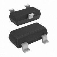
MOSFET N-CH 100V 150MA SOT-23
Manufacturer
NXP Semiconductors
Series
TrenchMOS™r
Type
Power MOSFETr
Datasheet
1.BSS123215.pdf
(4 pages)
Specifications of BSS123,215
Package / Case
SOT-23-3, TO-236-3, Micro3™, SSD3, SST3
Fet Type
MOSFET N-Channel, Metal Oxide
Fet Feature
Standard
Rds On (max) @ Id, Vgs
6 Ohm @ 120mA, 10V
Drain To Source Voltage (vdss)
100V
Current - Continuous Drain (id) @ 25° C
150mA
Vgs(th) (max) @ Id
2.8V @ 1mA
Input Capacitance (ciss) @ Vds
40pF @ 25V
Power - Max
250mW
Mounting Type
Surface Mount
Minimum Operating Temperature
- 55 C
Configuration
Single
Transistor Polarity
N-Channel
Resistance Drain-source Rds (on)
6 Ohm @ 10 V
Drain-source Breakdown Voltage
100 V
Gate-source Breakdown Voltage
+/- 20 V
Continuous Drain Current
0.15 A
Power Dissipation
250 mW
Maximum Operating Temperature
+ 150 C
Mounting Style
SMD/SMT
Number Of Elements
1
Polarity
N
Channel Mode
Enhancement
Drain-source On-res
6Ohm
Drain-source On-volt
100V
Gate-source Voltage (max)
±20V
Operating Temp Range
-55C to 150C
Operating Temperature Classification
Military
Mounting
Surface Mount
Pin Count
3
Package Type
TO-236AB
Lead Free Status / RoHS Status
Lead free / RoHS Compliant
Gate Charge (qg) @ Vgs
-
Lead Free Status / Rohs Status
Lead free / RoHS Compliant
Other names
568-4873-2
933946340215
BSS123 T/R
BSS123 T/R
BSS123,215
933946340215
BSS123 T/R
BSS123 T/R
BSS123,215
Available stocks
Company
Part Number
Manufacturer
Quantity
Price
Company:

Part Number:
BSS123,215
Manufacturer:
NXP Semiconductors
Quantity:
9 400


Philips Semiconductors
ELECTRICAL CHARACTERISTICS
T
August 2000
N-channel TrenchMOS
Logic level FET
SYMBOL PARAMETER
V
V
R
g
I
I
t
t
C
C
C
j
= 25˚C unless otherwise specified
DSS
GSS
on
off
fs
(BR)DSS
GS(TO)
DS(ON)
iss
oss
rss
Drain-source breakdown
voltage
Gate threshold voltage
Drain-source on-state
resistance
Forward transconductance
Zero gate voltage drain
current
Gate source leakage current V
Turn-on time
Turn-off time
Input capacitance
Output capacitance
Feedback capacitance
transistor
CONDITIONS
V
V
V
V
V
V
R
V
GS
DS
GS
DS
DS
GS
DD
GS
G
= 50 ; Resistive load
= 0 V; I
= V
= 10 V; I
= 25 V; I
= 60 V; V
= 20 V; V
= 50 V; R
= 0 V; V
GS
; I
D
D
DS
D
D
= 10 A
= 1 mA
GS
D
= 120 mA
= 120 mA
DS
2
= 25 V; f = 1 MHz
= 250 ; V
= 0 V
= 0 V
GS
= 10 V;
MIN.
100
1
-
-
-
-
-
-
-
-
-
TYP. MAX. UNIT
Product specification
130
350
3.5
10
10
12
23
2
3
6
4
100
100
2.8
10
20
40
25
10
BSS123
6
-
-
Rev 1.000
mS
nA
nA
pF
pF
pF
ns
ns
V
V
Related parts for BSS123,215
Image
Part Number
Description
Manufacturer
Datasheet
Request
R

Part Number:
Description:
Logic level N-channel enhancement mode Field-Effect Transistor (FET) in a plastic package using TrenchMOS technology
Manufacturer:
NXP Semiconductors
Datasheet:

Part Number:
Description:
NXP Semiconductors designed the LPC2420/2460 microcontroller around a 16-bit/32-bitARM7TDMI-S CPU core with real-time debug interfaces that include both JTAG andembedded trace
Manufacturer:
NXP Semiconductors
Datasheet:

Part Number:
Description:
NXP Semiconductors designed the LPC2458 microcontroller around a 16-bit/32-bitARM7TDMI-S CPU core with real-time debug interfaces that include both JTAG andembedded trace
Manufacturer:
NXP Semiconductors
Datasheet:
Part Number:
Description:
NXP Semiconductors designed the LPC2468 microcontroller around a 16-bit/32-bitARM7TDMI-S CPU core with real-time debug interfaces that include both JTAG andembedded trace
Manufacturer:
NXP Semiconductors
Datasheet:
Part Number:
Description:
NXP Semiconductors designed the LPC2470 microcontroller, powered by theARM7TDMI-S core, to be a highly integrated microcontroller for a wide range ofapplications that require advanced communications and high quality graphic displays
Manufacturer:
NXP Semiconductors
Datasheet:
Part Number:
Description:
NXP Semiconductors designed the LPC2478 microcontroller, powered by theARM7TDMI-S core, to be a highly integrated microcontroller for a wide range ofapplications that require advanced communications and high quality graphic displays
Manufacturer:
NXP Semiconductors
Datasheet:
Part Number:
Description:
The Philips Semiconductors XA (eXtended Architecture) family of 16-bit single-chip microcontrollers is powerful enough to easily handle the requirements of high performance embedded applications, yet inexpensive enough to compete in the market for hi
Manufacturer:
NXP Semiconductors
Datasheet:
Part Number:
Description:
The XA-S3 device is a member of Philips Semiconductors? XA(eXtended Architecture) family of high performance 16-bitsingle-chip microcontrollers
Manufacturer:
NXP Semiconductors
Datasheet:

Part Number:
Description:
The NXP BlueStreak LH75401/LH75411 family consists of two low-cost 16/32-bit System-on-Chip (SoC) devices
Manufacturer:
NXP Semiconductors
Datasheet:
Part Number:
Description:
The NXP LPC3130/3131 combine an 180 MHz ARM926EJ-S CPU core, high-speed USB2
Manufacturer:
NXP Semiconductors
Datasheet:
Part Number:
Description:
The NXP LPC3141 combine a 270 MHz ARM926EJ-S CPU core, High-speed USB 2
Manufacturer:
NXP Semiconductors
Part Number:
Description:
The NXP LPC3143 combine a 270 MHz ARM926EJ-S CPU core, High-speed USB 2
Manufacturer:
NXP Semiconductors

Part Number:
Description:
The NXP LPC3152 combines an 180 MHz ARM926EJ-S CPU core, High-speed USB 2
Manufacturer:
NXP Semiconductors
Part Number:
Description:
The NXP LPC3154 combines an 180 MHz ARM926EJ-S CPU core, High-speed USB 2
Manufacturer:
NXP Semiconductors