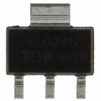
IRLL024NTRPBF International Rectifier, IRLL024NTRPBF Datasheet - Page 2
IRLL024NTRPBF
Manufacturer Part Number
IRLL024NTRPBF
Description
MOSFET N-CH 55V 3.1A SOT223
Manufacturer
International Rectifier
Series
HEXFET®r
Specifications of IRLL024NTRPBF
Fet Type
MOSFET N-Channel, Metal Oxide
Fet Feature
Logic Level Gate
Rds On (max) @ Id, Vgs
65 mOhm @ 3.1A, 10V
Drain To Source Voltage (vdss)
55V
Current - Continuous Drain (id) @ 25° C
3.1A
Vgs(th) (max) @ Id
2V @ 250µA
Gate Charge (qg) @ Vgs
15.6nC @ 5V
Input Capacitance (ciss) @ Vds
510pF @ 25V
Power - Max
1W
Mounting Type
Surface Mount
Package / Case
SOT-223 (3 leads + Tab), SC-73, TO-261
Current, Drain
4.4 A
Gate Charge, Total
10.4 nC
Package Type
SOT-223
Polarization
N-Channel
Power Dissipation
2.1 W
Resistance, Drain To Source On
0.065 Ohm
Temperature, Operating, Maximum
+150 °C
Temperature, Operating, Minimum
-55 °C
Time, Turn-off Delay
18 ns
Time, Turn-on Delay
7.4 ns
Transconductance, Forward
3.3 S
Voltage, Breakdown, Drain To Source
55 V
Voltage, Forward, Diode
1 V
Voltage, Gate To Source
±16 V
Transistor Polarity
N-Channel
Resistance Drain-source Rds (on)
100 mOhms
Drain-source Breakdown Voltage
55 V
Gate-source Breakdown Voltage
16 V
Continuous Drain Current
4.4 A
Mounting Style
SMD/SMT
Gate Charge Qg
10.4 nC
Lead Free Status / RoHS Status
Lead free / RoHS Compliant
Other names
IRLL024NPBFTR
IRLL024NTRPBF
IRLL024NTRPBFTR
IRLL024NTRPBF
IRLL024NTRPBFTR
Available stocks
Company
Part Number
Manufacturer
Quantity
Price

Part Number:
IRLL024NTRPBF
Manufacturer:
IR
Quantity:
20 000


Electrical Characteristics @ T
Source-Drain Ratings and Characteristics
‚
Notes:
IRLL024NPbF
I
I
V
t
Q
t
V
∆V
R
V
g
I
I
Q
Q
Q
t
t
t
t
C
C
C
S
SM
rr
on
DSS
GSS
d(on)
r
d(off)
f
SD
fs
2
rr
(BR)DSS
DS(on)
GS(th)
Repetitive rating; pulse width limited by
gs
gd
iss
oss
rss
Starting T
g
max. junction temperature. ( See fig. 11 )
R
(BR)DSS
G
= 25Ω, I
/∆T
J
J
= 25°C, L = 25 mH
Continuous Source Current
(Body Diode)
Pulsed Source Current
(Body Diode)
Diode Forward Voltage
Reverse Recovery Time
Reverse RecoveryCharge
Forward Turn-On Time
Drain-to-Source Breakdown Voltage
Breakdown Voltage Temp. Coefficient
Static Drain-to-Source On-Resistance
Gate Threshold Voltage
Forward Transconductance
Drain-to-Source Leakage Current
Gate-to-Source Forward Leakage
Gate-to-Source Reverse Leakage
Total Gate Charge
Gate-to-Source Charge
Gate-to-Drain ("Miller") Charge
Turn-On Delay Time
Rise Time
Turn-Off Delay Time
Fall Time
Input Capacitance
Output Capacitance
Reverse Transfer Capacitance
AS
= 3.1A. (See Figure 12)
Parameter
Parameter
J
= 25°C (unless otherwise specified)
ƒ
„
Pulse width ≤ 300µs; duty cycle ≤ 2%.
I
T
SD
–––
Min. Typ. Max. Units
–––
––– 0.048 –––
–––
–––
–––
–––
–––
–––
–––
–––
–––
–––
–––
–––
–––
–––
–––
–––
Min. Typ. Max. Units
1.0
3.3
–––
–––
–––
–––
55
J
Intrinsic turn-on time is negligible (turn-on is dominated by L
≤ 150°C
≤ 1.9A, di/dt ≤ 270A/µs, V
–––
–––
10.4 15.6
–––
–––
––– 0.065
––– 0.080
––– 0.100
–––
–––
–––
–––
–––
510
140
––– -100
39
63
1.5
5.5
7.4
21
18
25
58
100
–––
–––
–––
–––
–––
12
1.0
–––
–––
250
–––
–––
3.1
58
94
2.0
2.3
8.3
25
V/°C
nC
ns
µA
nA
nC
ns
pF
V
Ω
A
V
V
S
MOSFET symbol
showing the
integral reverse
p-n junction diode.
T
T
di/dt = 100A/µs „
V
Reference to 25°C, I
V
V
V
V
V
V
V
V
I
V
V
V
I
R
R
V
V
ƒ = 1.0MHz, See Fig. 5
V
D
D
J
J
DD
GS
GS
GS
GS
DS
DS
DS
DS
GS
GS
DS
GS
DD
GS
DS
G
D
= 25°C, I
= 25°C, I
= 1.9A
= 1.9A
= 15 Ω, See Fig. 10 „
= 24 Ω
≤ V
= 0V, I
= 10V, I
= V
= 25V, I
= 55V, V
= 44V, V
= 16V
= -16V
= 44V
= 28V
= 0V
= 25V
= 5.0V, I
= 4.0V, I
= 5.0V, See Fig. 6 and 9 „
(BR)DSS
GS
, I
D
S
F
D
D
D
Conditions
= 250µA
D
D
= 1.9A
GS
GS
= 1.9A, V
Conditions
= 250µA
= 1.9 A
,
= 3.1A „
= 2.5A „
= 1.6A „
= 0V
= 0V, T
D
= 1mA
GS
J
= 125°C
= 0V „
S
+L
D
)
Related parts for IRLL024NTRPBF
Image
Part Number
Description
Manufacturer
Datasheet
Request
R

Part Number:
Description:
Manufacturer:
International Rectifier Corp.
Datasheet:
Part Number:
Description:
SCHOTTKY RECTIFIER
Manufacturer:
International Rectifier Corp.
Datasheet:
Part Number:
Description:
SCHOTTKY RECTIFIER
Manufacturer:
International Rectifier Corp.
Datasheet:
Part Number:
Description:
SCHOTTKY RECTIFIER
Manufacturer:
International Rectifier Corp.
Datasheet:
Part Number:
Description:
SCHOTTKY RECTIFIER
Manufacturer:
International Rectifier Corp.
Datasheet:
Part Number:
Description:
SCHOTTKY RECTIFIER
Manufacturer:
International Rectifier Corp.
Datasheet:
Part Number:
Description:
SCHOTTKY RECTIFIER
Manufacturer:
International Rectifier Corp.
Datasheet:
Part Number:
Description:
SCHOTTKY RECTIFIER
Manufacturer:
International Rectifier Corp.
Datasheet:
Part Number:
Description:
SCHOTTKY RECTIFIER
Manufacturer:
International Rectifier Corp.
Datasheet:
Part Number:
Description:
SCHOTTKY RECTIFIER
Manufacturer:
International Rectifier Corp.
Datasheet:
Part Number:
Description:
SCHOTTKY RECTIFIER
Manufacturer:
International Rectifier Corp.
Datasheet:
Part Number:
Description:
SCHOTTKY RECTIFIER
Manufacturer:
International Rectifier Corp.
Datasheet:
Part Number:
Description:
SCHOTTKY RECTIFIER
Manufacturer:
International Rectifier Corp.
Datasheet:
Part Number:
Description:
SCHOTTKY RECTIFIER
Manufacturer:
International Rectifier Corp.
Datasheet:
Part Number:
Description:
SCHOTTKY RECTIFIER
Manufacturer:
International Rectifier Corp.
Datasheet: