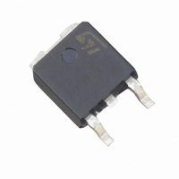
STD15NF10T4 STMicroelectronics, STD15NF10T4 Datasheet - Page 4

STD15NF10T4
Manufacturer Part Number
STD15NF10T4
Description
MOSFET N-CH 100V 23A DPAK
Manufacturer
STMicroelectronics
Series
STripFET™r
Datasheet
1.STD15NF10T4.pdf
(13 pages)
Specifications of STD15NF10T4
Fet Type
MOSFET N-Channel, Metal Oxide
Fet Feature
Standard
Rds On (max) @ Id, Vgs
65 mOhm @ 12A, 10V
Drain To Source Voltage (vdss)
100V
Current - Continuous Drain (id) @ 25° C
23A
Vgs(th) (max) @ Id
4V @ 250µA
Gate Charge (qg) @ Vgs
40nC @ 10V
Input Capacitance (ciss) @ Vds
870pF @ 25V
Power - Max
70W
Mounting Type
Surface Mount
Package / Case
DPak, TO-252 (2 leads+tab), SC-63
Configuration
Single
Transistor Polarity
N-Channel
Resistance Drain-source Rds (on)
0.08 Ohm @ 10 V
Forward Transconductance Gfs (max / Min)
12 S
Drain-source Breakdown Voltage
100 V
Gate-source Breakdown Voltage
+/- 20 V
Continuous Drain Current
23 A
Power Dissipation
70000 mW
Maximum Operating Temperature
+ 175 C
Mounting Style
SMD/SMT
Minimum Operating Temperature
- 55 C
Lead Free Status / RoHS Status
Lead free / RoHS Compliant
Other names
497-7958-2
STD15NF10T4
STD15NF10T4
Available stocks
Company
Part Number
Manufacturer
Quantity
Price
Company:
Part Number:
STD15NF10T4
Manufacturer:
ST
Quantity:
15 000
Part Number:
STD15NF10T4
Manufacturer:
ST
Quantity:
20 000
Electrical characteristics
2
4/13
Electrical characteristics
(T
Table 4.
1.
Table 5.
1. Pulsed: pulse duration=300µs, duty cycle 1.5%
Table 6.
V
Symbol
Symbol
Symbol
R
CASE
V
(BR)DSS
g
t
t
C
I
I
DS(on)
C
C
GS(th)
Q
Q
d(on)
d(off)
Pulsed: Pulse duration = 300 µs, duty cycle 1.5%
DSS
GSS
fs
Q
oss
t
t
rss
iss
gs
gd
r
f
g
(1)
= 25 °C unless otherwise specified)
Forward transconductance
Input capacitance
Output capacitance
Reverse transfer
capacitance
Total gate charge
Gate-source charge
Gate-drain charge
Turn-on delay time
Rise time
Turn-off delay time
Fall time
Drain-source breakdown
voltage
Zero gate voltage drain
current (V
Gate body leakage current
(V
Gate threshold voltage
Static drain-source on
resistance
On
Dynamic
Switching times
DS
(1)
= 0)
/off states
Parameter
Parameter
Parameter
GS
= 0)
I
V
V
V
V
V
V
V
V
V
V
V
R
Figure 13 on page 8
D
DS
DS
GS
DS
GS
GS
GS
DS
DS
DD
DD
G
= 250 µA, V
= 4.7 Ω, V
= V
= Max rating
= Max rating,@ 125 °C
= ± 20 V
= 10 V, I
= 25 V, f = 1 MHz,
= 0
= 10 V
= 15 V
= 80 V, I
= 50 V, I
Test conditions
Test conditions
Test conditions
GS
, I
,
D
I
D
D
D
D
= 250 µA
GS
GS
= 12 A
= 7.5 A
= 24 A
= 12 A,
= 10 V
= 0
Min.
Min.
Min.
100
2
Typ.
Typ.
0.06
870
125
Typ.
12
50
30
10
60
45
49
17
6
3
Max.
0.065
STD15NF10
Max.
±100
Max.
40
10
1
4
Unit
Unit
Unit
nC
nC
nC
pF
pF
pF
µA
µA
nA
ns
ns
ns
ns
S
V
V
Ω


