IRF3710LPBF International Rectifier, IRF3710LPBF Datasheet - Page 2
IRF3710LPBF
Manufacturer Part Number
IRF3710LPBF
Description
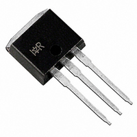
MOSFET N-CH 100V 57A TO-262
Manufacturer
International Rectifier
Series
HEXFET®r
Datasheet
1.IRF3710LPBF.pdf
(10 pages)
Specifications of IRF3710LPBF
Fet Type
MOSFET N-Channel, Metal Oxide
Fet Feature
Standard
Rds On (max) @ Id, Vgs
23 mOhm @ 28A, 10V
Drain To Source Voltage (vdss)
100V
Current - Continuous Drain (id) @ 25° C
57A
Vgs(th) (max) @ Id
4V @ 250µA
Gate Charge (qg) @ Vgs
130nC @ 10V
Input Capacitance (ciss) @ Vds
3130pF @ 25V
Power - Max
200W
Mounting Type
Through Hole
Package / Case
TO-262-3 (Straight Leads)
Transistor Polarity
N-Channel
Drain-source Breakdown Voltage
100 V
Gate-source Breakdown Voltage
20 V
Continuous Drain Current
57 A
Power Dissipation
200 W
Mounting Style
Through Hole
Gate Charge Qg
86.7 nC
Lead Free Status / RoHS Status
Lead free / RoHS Compliant
Other names
*IRF3710LPBF


Source-Drain Ratings and Characteristics
Electrical Characteristics @ T
‚
ƒ
„
Notes:
V
∆V
R
V
g
I
I
Q
Q
Q
t
t
t
t
C
C
C
E
L
L
I
I
V
t
Q
t
DSS
GSS
SM
d(on)
r
d(off)
f
S
rr
on
2
fs
D
S
(BR)DSS
GS(th)
AS
SD
DS(on)
g
gs
gd
iss
oss
rss
rr
Repetitive rating; pulse width limited by
Pulse width ≤ 400µs; duty cycle ≤ 2%.
I
(BR)DSS
T
max. junction temperature. (See fig. 11).
Starting T
AS
J
≤ 175°C.
= 28A, V
≤ 28A di/d ≤ 380A/µs, V
/∆T
J
J
Drain-to-Source Leakage Current
Drain-to-Source Breakdown Voltage
Breakdown Voltage Temp. Coefficient
Static Drain-to-Source On-Resistance
Gate Threshold Voltage
Forward Transconductance
Gate-to-Source Forward Leakage
Gate-to-Source Reverse Leakage
Total Gate Charge
Gate-to-Source Charge
Gate-to-Drain ("Miller") Charge
Turn-On Delay Time
Rise Time
Turn-Off Delay Time
Fall Time
Input Capacitance
Output Capacitance
Reverse Transfer Capacitance
Single Pulse Avalanche Energy
Continuous Source Current
(Body Diode)
Pulsed Source Current
(Body Diode)
Diode Forward Voltage
Reverse Recovery Time
Reverse Recovery Charge
Forward Turn-On Time
Internal Drain Inductance
Internal Source Inductance
= 25°C, L = 0.70mH, R
GS
=10V. (See Figure 12).
Parameter
Parameter
DD
≤ V
G
(BR)DSS
= 25Ω,
J
,
= 25°C (unless otherwise specified)
‚‡
…
†
‡
**When mounted on 1" square PCB (FR-4 or G-10 Material). For
recommended footprint and soldering techniques refer to application
note #AN-994.
This is a typical value at device destruction and represents
This is a calculated value limited to T
Uses IRF3710 data and test conditions.
operation outside rated limits.
100
–––
–––
–––
–––
–––
–––
–––
–––
–––
–––
–––
–––
–––
–––
–––
––– 1060…280†
–––
–––
Min. Typ. Max. Units
2.0
Min. Typ. Max. Units
32
–––
–––
–––
–––
–––
–––
Intrinsic turn-on time is negligible (turn-on is dominated by L
3130 –––
0.13
–––
–––
–––
–––
–––
–––
–––
––– -100
–––
–––
–––
410
670 1010
–––
–––
–––
140
4.5
12
58
45
47
7.5
72
–––
–––
–––
–––
250
100
130
–––
–––
–––
–––
–––
–––
–––
220
4.0
1.2
23
25
26
43
230
57
V/°C
mΩ
µA
nA
nC
ns
nH
mJ
nC
pF
ns
V
V
S
V
V
Reference to 25°C, I
V
V
V
V
V
V
V
I
V
V
V
I
R
V
Between lead,
6mm (0.25in.)
from package
and center of die contact
V
V
ƒ = 1.0MHz, See Fig. 5‡
I
MOSFET symbol
showing the
integral reverse
p-n junction diode.
T
T
di/dt = 100A/µs
D
D
AS
GS
GS
DS
DS
DS
DS
GS
GS
DS
GS
DD
GS
GS
DS
J
J
G
= 28A
= 28A
= 25°C, I
= 25°C, I
= 28A, L = 0.70mH
= 2.5Ω
= 0V, I
= 10V, I
= V
= 25V, I
= 100V, V
= 80V, V
= 20V
= -20V
= 80V
= 10V, See Fig. 6 and 13‡
= 50V
= 10V, See Fig. 10 „‡
= 0V
= 25V
GS
J
, I
= 175°C .
D
S
F
D
D
D
Conditions
= 250µA
Conditions
GS
= 28A
= 28A, V
=28A
= 250µA
= 28A„‡
GS
„
= 0V, T
= 0V
D
www.irf.com
„
GS
= 1mA‡
J
= 150°C
= 0V
G
G
S
„
+L
D
S
D
)
S
D
Related parts for IRF3710LPBF
Image
Part Number
Description
Manufacturer
Datasheet
Request
R

Part Number:
Description:
Manufacturer:
International Rectifier Corp.
Datasheet:

Part Number:
Description:
Common Mode Inductors (Chokes) 5.6uH 10%
Manufacturer:
Vishay
Datasheet:
Part Number:
Description:
Common Mode Inductors (Chokes) 10uH 10%
Manufacturer:
Vishay
Datasheet:
Part Number:
Description:
SCHOTTKY RECTIFIER
Manufacturer:
International Rectifier Corp.
Datasheet:
Part Number:
Description:
SCHOTTKY RECTIFIER
Manufacturer:
International Rectifier Corp.
Datasheet:
Part Number:
Description:
SCHOTTKY RECTIFIER
Manufacturer:
International Rectifier Corp.
Datasheet:
Part Number:
Description:
SCHOTTKY RECTIFIER
Manufacturer:
International Rectifier Corp.
Datasheet:
Part Number:
Description:
SCHOTTKY RECTIFIER
Manufacturer:
International Rectifier Corp.
Datasheet:
Part Number:
Description:
SCHOTTKY RECTIFIER
Manufacturer:
International Rectifier Corp.
Datasheet:
Part Number:
Description:
SCHOTTKY RECTIFIER
Manufacturer:
International Rectifier Corp.
Datasheet:
Part Number:
Description:
SCHOTTKY RECTIFIER
Manufacturer:
International Rectifier Corp.
Datasheet:
Part Number:
Description:
SCHOTTKY RECTIFIER
Manufacturer:
International Rectifier Corp.
Datasheet:
Part Number:
Description:
SCHOTTKY RECTIFIER
Manufacturer:
International Rectifier Corp.
Datasheet:
Part Number:
Description:
SCHOTTKY RECTIFIER
Manufacturer:
International Rectifier Corp.
Datasheet:
Part Number:
Description:
SCHOTTKY RECTIFIER
Manufacturer:
International Rectifier Corp.
Datasheet: