STV160NF03LT4 STMicroelectronics, STV160NF03LT4 Datasheet - Page 3
STV160NF03LT4
Manufacturer Part Number
STV160NF03LT4
Description
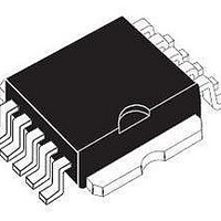
MOSFET N-CH 30V 160A POWERSO-10
Manufacturer
STMicroelectronics
Series
STripFET™r
Datasheet
1.STV160NF03LT4.pdf
(9 pages)
Specifications of STV160NF03LT4
Fet Type
MOSFET N-Channel, Metal Oxide
Fet Feature
Logic Level Gate
Rds On (max) @ Id, Vgs
2.8 mOhm @ 80A, 10V
Drain To Source Voltage (vdss)
30V
Current - Continuous Drain (id) @ 25° C
160A
Vgs(th) (max) @ Id
1V @ 250µA
Gate Charge (qg) @ Vgs
140nC @ 10V
Input Capacitance (ciss) @ Vds
4700pF @ 25V
Power - Max
210W
Mounting Type
Surface Mount
Package / Case
PowerSO-10 Exposed Bottom Pad
Configuration
Single
Transistor Polarity
N-Channel
Resistance Drain-source Rds (on)
0.0019 Ohms
Forward Transconductance Gfs (max / Min)
210 S
Drain-source Breakdown Voltage
30 V
Gate-source Breakdown Voltage
+/- 15 V
Continuous Drain Current
160 A
Power Dissipation
210 W
Maximum Operating Temperature
+ 175 C
Mounting Style
SMD/SMT
Minimum Operating Temperature
- 65 C
Lead Free Status / RoHS Status
Lead free / RoHS Compliant
Other names
497-3252-2
Available stocks
Company
Part Number
Manufacturer
Quantity
Price

Part Number:
STV160NF03LT4
Manufacturer:
ST
Quantity:
20 000


ELECTRICAL CHARACTERISTICS (CONTINUED)
SWITCHING ON
SWITCHING OFF
SOURCE DRAIN DIODE
Note: 1. Pulsed: Pulse duration = 300 µs, duty cycle 1.5 %.
Safe Operating Area
Symbol
Symbol
Symbol
I
V
SDM
t
t
t
t
I
SD
r(Voff)
d(on)
Q
Q
d(off)
d(off)
RRM
I
2. Pulse width limited by safe operating area.
Q
Q
SD
t
t
t
t
t
rr
gd
r
gs
c
f
f
g
rr
(2)
(1)
Turn-on Delay Time
Rise Time
Total Gate Charge
Gate-Source Charge
Gate-Drain Charge
Source-drain Current
Source-drain Current (pulsed)
Forward On Voltage
Reverse Recovery Time
Reverse Recovery Charge
Reverse Recovery Current
Turn-off-Delay Time
Fall Time
Turn-off Delay Time
Off-voltage Rise Time
Fall Time
Cross-over Time
Parameter
Parameter
Parameter
V
R
(see test circuit, Figure 3)
V
I
I
V
(see test circuit, Figure 5)
V
V
R
(see test circuit, Figure 5)
Vclamp = 24 V, I
R
SD
SD
DD
G
DD
GS
DD
DD
G
G
= 4.7
= 4.7
= 4.7
= 160 A, V
= 80 A, di/dt = 100A/µs,
= 15 V, I
= 24 V, I
= 10 V
= 15 V, I
= 15V, T
Test Conditions
Test Conditions
Test Conditions
V
V
V
GS
D
D
D
j
GS
GS
= 25°C
GS
= 80 A
= 160 A,
= 80 A,
= 10V
= 10 V
D
= 10V
Thermal Impedance
= 0
= 40 A
Min.
Min.
Min.
Typ.
Typ.
Typ.
380
103
180
170
125
4.5
30
80
21
38
80
75
25
90
STV160NF03L
Max.
Max.
Max.
140
160
640
1.5
Unit
Unit
Unit
nC
nC
nC
nC
ns
ns
ns
ns
ns
ns
ns
ns
ns
A
A
V
A
3/9
Related parts for STV160NF03LT4
Image
Part Number
Description
Manufacturer
Datasheet
Request
R

Part Number:
Description:
STMicroelectronics [RIPPLE-CARRY BINARY COUNTER/DIVIDERS]
Manufacturer:
STMicroelectronics
Datasheet:
Part Number:
Description:
STMicroelectronics [LIQUID-CRYSTAL DISPLAY DRIVERS]
Manufacturer:
STMicroelectronics
Datasheet:

Part Number:
Description:
BOARD EVAL FOR MEMS SENSORS
Manufacturer:
STMicroelectronics
Datasheet:
Part Number:
Description:
NPN TRANSISTOR POWER MODULE
Manufacturer:
STMicroelectronics
Datasheet:
Part Number:
Description:
TURBOSWITCH ULTRA-FAST HIGH VOLTAGE DIODE
Manufacturer:
STMicroelectronics
Datasheet:
Part Number:
Description:
Manufacturer:
STMicroelectronics
Datasheet:
Part Number:
Description:
DIODE / SCR MODULE
Manufacturer:
STMicroelectronics
Datasheet:
Part Number:
Description:
DIODE / SCR MODULE
Manufacturer:
STMicroelectronics
Datasheet:
Part Number:
Description:
Search -----> STE16N100
Manufacturer:
STMicroelectronics
Datasheet:
Part Number:
Description:
Search ---> STE53NA50
Manufacturer:
STMicroelectronics
Datasheet:
Part Number:
Description:
NPN Transistor Power Module
Manufacturer:
STMicroelectronics
Datasheet:
Part Number:
Description:
DIODE / SCR MODULE
Manufacturer:
STMicroelectronics
Datasheet: