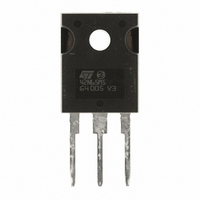
STW42N65M5 STMicroelectronics, STW42N65M5 Datasheet - Page 5

STW42N65M5
Manufacturer Part Number
STW42N65M5
Description
MOSFET N-CH 650V 33A TO-247
Manufacturer
STMicroelectronics
Series
MDmesh™r
Datasheet
1.STP42N65M5.pdf
(18 pages)
Specifications of STW42N65M5
Fet Type
MOSFET N-Channel, Metal Oxide
Fet Feature
Standard
Rds On (max) @ Id, Vgs
79 mOhm @ 16.5A, 10V
Drain To Source Voltage (vdss)
650V
Current - Continuous Drain (id) @ 25° C
33A
Vgs(th) (max) @ Id
5V @ 250µA
Gate Charge (qg) @ Vgs
100nC @ 10V
Input Capacitance (ciss) @ Vds
4650pF @ 100V
Power - Max
190W
Mounting Type
Through Hole
Package / Case
TO-247
Transistor Polarity
N Channel
Continuous Drain Current Id
33A
Drain Source Voltage Vds
650V
On Resistance Rds(on)
0.07ohm
Rds(on) Test Voltage Vgs
10V
Threshold Voltage Vgs Typ
4V
Configuration
Single
Resistance Drain-source Rds (on)
0.07 Ohms
Drain-source Breakdown Voltage
650 V
Gate-source Breakdown Voltage
+/- 25 V
Continuous Drain Current
33 A
Power Dissipation
190 W
Maximum Operating Temperature
+ 150 C
Mounting Style
Through Hole
Minimum Operating Temperature
- 55 C
Lead Free Status / RoHS Status
Lead free / RoHS Compliant
Other names
497-8796-5
Available stocks
Company
Part Number
Manufacturer
Quantity
Price
Company:
Part Number:
STW42N65M5
Manufacturer:
FSC
Quantity:
6 000
Part Number:
STW42N65M5
Manufacturer:
ST
Quantity:
20 000
STx42N65M5
Table 6.
Table 7.
1. Pulse width limited by safe operating area
2. Pulsed: Pulse duration = 300 µs, duty cycle 1.5%
Symbol
Symbol
I
V
SDM
t
t
I
I
SD
d(on)
d(off)
RRM
RRM
I
Q
Q
SD
t
t
t
t
rr
rr
r
f
rr
rr
(2)
(1)
Turn-on delay time
Rise time
Turn-off-delay time
Fall time
Source-drain current
Source-drain current (pulsed)
Forward on voltage
Reverse recovery time
Reverse recovery charge
Reverse recovery current
Reverse recovery time
Reverse recovery charge
Reverse recovery current
Switching times
Source drain diode
Parameter
Parameter
Doc ID 15317 Rev 3
V
R
(see
DD
G
= 4.7 Ω, V
= 400 V, I
Figure
I
I
V
I
V
(see
SD
SD
SD
Test conditions
DD
DD
= 33 A, V
= 33 A, di/dt = 100 A/µs
= 33 A, di/dt = 100 A/µs
= 100 V (see
= 100 V, T
Figure
19)
Test conditions
GS
D
= 20 A,
= 10 V
24)
GS
j
= 150 °C
= 0
Figure
24)
Min.
Electrical characteristics
-
Min.
-
-
-
-
Typ.
61
24
65
13
Typ. Max. Unit
400
532
35
10
38
7
Max
132
1.5
33
-
Unit
µC
µC
ns
ns
ns
ns
ns
ns
A
A
V
A
A
5/18


