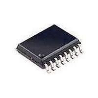
GTL2009PW NXP Semiconductors, GTL2009PW Datasheet - Page 5

GTL2009PW
Manufacturer Part Number
GTL2009PW
Description
Comparator ICs 3-BIT FSB FREQ CMPR
Manufacturer
NXP Semiconductors
Datasheet
1.GTL2009PW118.pdf
(17 pages)
Specifications of GTL2009PW
Number Of Channels
3 Channels
Comparator Type
Magnitude
Product
Digital Comparators
Output Type
Complementary
Supply Voltage (max)
3.6 V
Supply Voltage (min)
3 V
Supply Current (max)
10 mA
Maximum Operating Temperature
85 C
Mounting Style
SMD/SMT
Package / Case
SOT-403
Minimum Operating Temperature
- 40 C
Lead Free Status / RoHS Status
Lead free / RoHS Compliant
Other names
GTL2009PW,112
Available stocks
Company
Part Number
Manufacturer
Quantity
Price
Part Number:
GTL2009PW
Manufacturer:
PHILIPS/飞利浦
Quantity:
20 000
Philips Semiconductors
9397 750 13556
Product data sheet
7.2 Default conditions input
The FSB GTL output data is masked and a specific default value (100 MHz) is inserted
upon power-up when V
and valid data is supplied when the VREF input crosses a static 0.6 V internally generated
input comparator reference voltage. For slowly rising GTL V
switch-over happens at the 0.6 V threshold. For fast rising GTL V
the switch-over typically occurs between 350 ns to 1.5 s after the 0.6 V threshold is
exceeded.
The AO1 and AO2 outputs do not have ‘default conditions’ like those assigned to the GTL
outputs. Instead, these two pins will power-up according to the conditions applied to the
1A1 and 2A1 input pins as shown in
Table 8:
H = HIGH; L = LOW.
It is important to note that the AO1 and AO2 outputs may be valid a little before 1.5 V and
will rise with V
V
GTL2009. No firm answer for this can be given since the time it takes for V
regulation varies from 100 ms to 1000 ms, and the rise time of V
GTL2009 outputs are valid after the GTL inputs are valid plus 19.6 ns (worst-case
propagation delay of the GTL-to-LVTTL path).
1AI
L
L
L
L
H
H
H
H
DD
is in regulation, V
AO1 and AO2 power-up conditions
DD
. Valid outputs from the system level perspective will be achieved after
2AI
L
L
H
H
L
L
H
H
Rev. 01 — 22 September 2005
TT
DD
ramps up, and after the internal propagation delay of the
is greater than 1.5 V. The FSB GTL output data is unmasked
V
<1.5 V
>1.5 V
<1.5 V
>1.5 V
<1.5 V
>1.5 V
<1.5 V
>1.5 V
Table
DD
3-bit GTL Front-Side Bus frequency comparator
8. If the slot is occupied, the input is LOW.
AO1
L
H
L
L
L
L
L
H
© Koninklijke Philips Electronics N.V. 2005. All rights reserved.
TT
supply (0.7 V/500 s), the
TT
TT
supply (0.7 V/100 ns),
is unknown. The
GTL2009
AO2
L
H
L
L
L
H
L
H
DD
to be in
5 of 17


