TOSHIBA DTMOS II FAMILY OF 600V POWER MOSFETS USE SUPERJUNCTION...
http://www.toshiba.com/taec/news/press_releases/2008/power_08_538.jsp
IRVINE, Calif., Sept. 3, 2008 — Toshiba America
Electronic Components, Inc. (TAEC)* today announced
a family of 600V DTMOS II superjunction MOSFETs
that contribute to higher efficiency of switched-mode
power supplies, such as AC adapters in notebook and
desktop computers, servers, flat panel displays, and
ballasts used in lighting, due to lower on-state
resistance (R
characteristics. Developed by Toshiba Corp., the
DTMOS II MOSFETs employ a superjunction structure
that enables a reduction in both on-state resistance
(R
tradeoffs. Typically, when either of these
characteristics is reduced, the other increases, but with
its superjunction DTMOS II design, Toshiba has been
able to reduce both simultaneously, enabling higher
power efficiency and switching performance than
conventional MOSFETs.
In these devices, Toshiba refined the superjunction
structure with the company's second generation
DTMOS technology. By applying this design and
optimizing the entire device, Toshiba has achieved
figure of merit values for R
that are approximately 68 percent less than that of
conventional Toshiba MOSFETs. This figure of merit is
one important performance index for MOSFETs in
which smaller is better, and is indicative of higher
switching performance and power efficiency.
The first twelve products in the DTMOS II family include 12A, 15A, and 20A 600V MOSFETs, each offered
in a choice of four packages, including TO-3P(N), TO-220SIS, TO-220(W) and TFP, a compact surface
mount package. The 12A devices feature low on-resistance of 0.4 ohms ( Ω, max.), the 15A devices feature
on-resistance of 0.3 Ω (max.) and 20A devices have on-resistance rated at 0.19 Ω (max.).
"With a combination of low on-resistance, fast switching and ruggedness, our new DTMOS II devices are
ideally suited for the switched-mode power supply and ballast lighting markets and are expected to enable a
significant increase in power efficiency," said Jeff Lo, business development manager, Discrete Power
Devices, for TAEC.
Features
Technical Specifications:
12A, 15A, or 20A 600V MOSFETs in Second DTMOS Generation Utilize "Superjunction" Technology to Reduce
TOSHIBA DTMOS II FAMILY OF 600V POWER MOSFETS USE SUPERJUNCTION STRUCTURE
Part
Number
TK20J60U
TK20A60U
TK20D60U
On-state Resistance x Gate Charge by 68 Percent Compared to Conventional Toshiba MOSFET Technology
DS(ON)
Due to the superjunction structure, R
Based on R
MOSFETs available in the market today.
Available in four packages to provide designers a choice best suited to their needs: TO-3P(N), TO-220(W), TO-220SIS, or
TFP, a compact Toshiba package.
) and gate charge (Q
DS(ON)
Voltage
+ 30V
Source
(max.)
Gate-
V
DS(ON)
DSS
) and faster switching
* Q g, the Toshiba DTMOS II MOSFETs feature competitive performance among superjunction
Current
20A
(max.)
Drain
DS(ON)
I
D
g
Family/Line/Product Name
), which usually are
* Q g (see note 1)
resistance
0.19 Ω
R
(max.)
source
Drain-
DS(ON)
ON
TO INCREASE POWER EFFICIENCY
DS(ON)
2
Charge,
27nC
(typ.)
can be as low as 0.19 W (max.) for the 20A devices, at V
Gate
Q
g
3
Avalanche Energy
(mJ)
Single
Pulse
144
144
144
Download Larger Image (JPG 147KB)
Download Larger Image (JPG 147KB)
4
Repetitive
19
4
19
5
Package
Package/Dimensions
15.9 x 23.3 x 4.8
10 x 17.8 x 4.5
10 x 17.8 x 4.5
TO-220SIS
TO-220(W)
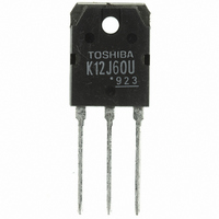
TO-3P(N)
Toshiba
(mm)
Industry
Standard
Equivalent
TO-247AD Sept. ‘08
(Isolated)
(Non-
isolated)
TO-220F
TO-220
DS
= 600V.
Planned
Mass
Production
Sept. ‘08
Sept. ‘08
Page 1 of 3
12/30/2008