BSS123LT1G ON Semiconductor, BSS123LT1G Datasheet - Page 2
BSS123LT1G
Manufacturer Part Number
BSS123LT1G
Description
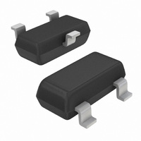
MOSFET N-CH 100V 170MA SOT-23
Manufacturer
ON Semiconductor
Type
Power MOSFETr
Specifications of BSS123LT1G
Fet Type
MOSFET N-Channel, Metal Oxide
Fet Feature
Logic Level Gate
Rds On (max) @ Id, Vgs
6 Ohm @ 100mA, 10V
Drain To Source Voltage (vdss)
100V
Current - Continuous Drain (id) @ 25° C
170mA
Vgs(th) (max) @ Id
2.8V @ 1mA
Input Capacitance (ciss) @ Vds
20pF @ 25V
Power - Max
225mW
Mounting Type
Surface Mount
Package / Case
SOT-23-3, TO-236-3, Micro3™, SSD3, SST3
Configuration
Single
Transistor Polarity
N-Channel
Resistance Drain-source Rds (on)
6 Ohm @ 10 V
Forward Transconductance Gfs (max / Min)
0.08 S
Drain-source Breakdown Voltage
100 V
Gate-source Breakdown Voltage
+/- 20 V
Continuous Drain Current
0.17 A
Power Dissipation
225 mW
Maximum Operating Temperature
+ 150 C
Mounting Style
SMD/SMT
Minimum Operating Temperature
- 55 C
Current, Drain
0.17 A
Package Type
SOT-23 (TO-236)
Polarization
N-Channel
Resistance, Drain To Source On
5 Ohms
Temperature, Operating, Maximum
+150 °C
Temperature, Operating, Minimum
-55 °C
Time, Turn-off Delay
40 ns
Time, Turn-on Delay
20 ns
Transconductance, Forward
80 Millimhos
Voltage, Breakdown, Drain To Source
100 V
Voltage, Forward, Diode
1.3 V
Voltage, Gate To Source
±20 VDC
Number Of Elements
1
Polarity
N
Channel Mode
Enhancement
Drain-source On-res
6Ohm
Drain-source On-volt
100V
Gate-source Voltage (max)
±20V
Drain Current (max)
170mA
Output Power (max)
Not RequiredW
Frequency (max)
Not RequiredMHz
Noise Figure
Not RequireddB
Power Gain
Not RequireddB
Drain Efficiency
Not Required%
Operating Temp Range
-55C to 150C
Operating Temperature Classification
Military
Mounting
Surface Mount
Pin Count
3
Lead Free Status / RoHS Status
Lead free / RoHS Compliant
Gate Charge (qg) @ Vgs
-
Lead Free Status / Rohs Status
Lead free / RoHS Compliant
Other names
BSS123LT1GOSTR
Available stocks
Company
Part Number
Manufacturer
Quantity
Price
Company:

Part Number:
BSS123LT1G
Manufacturer:
ON
Quantity:
60 000
Company:
Part Number:
BSS123LT1G
Manufacturer:
ON Semiconductor
Quantity:
20 000
Company:
Part Number:
BSS123LT1G
Manufacturer:
ON
Quantity:
30 000
Part Number:
BSS123LT1G
Manufacturer:
ON/安森美
Quantity:
20 000


4. Pulse Test: Pulse Width v 300 ms, Duty Cycle v 2.0%.
†For information on tape and reel specifications, including part orientation and tape sizes, please refer to our Tape and Reel Packaging
ELECTRICAL CHARACTERISTICS
OFF CHARACTERISTICS
ON CHARACTERISTICS
DYNAMIC CHARACTERISTICS
SWITCHING CHARACTERISTICS
REVERSE DIODE
ORDERING INFORMATION
Specifications Brochure, BRD8011/D.
Drain−Source Breakdown Voltage
Zero Gate Voltage Drain Current
Gate−Body Leakage Current
Gate Threshold Voltage
Static Drain−Source On−Resistance
Forward Transconductance
Input Capacitance
Output Capacitance
Reverse Transfer Capacitance
Turn−On Delay Time
Turn−Off Delay Time
Diode Forward On−Voltage
BSS123LT1
BSS123LT1G
BSS123LT3
BSS123LT3G
(V
(V
(V
(V
(V
(V
(V
(V
(V
(I
D
GS
GS
GS
DS
GS
DS
DS
DS
DS
= 0.34 Adc, V
= 0, I
= 0, V
= 20 Vdc, V
= V
= 10 Vdc, I
= 25 Vdc, I
= 25 Vdc, V
= 25 Vdc, V
= 25 Vdc, V
GS
D
DS
, I
= 250 mAdc)
D
= 100 Vdc)
= 1.0 mAdc)
D
D
GS
DS
GS
GS
GS
= 100 mAdc)
= 100 mAdc)
= 0 Vdc)
= 0)
= 0, f = 1.0 MHz)
= 0, f = 1.0 MHz)
= 0, f = 1.0 MHz)
Device
(Note 4)
T
T
J
J
= 25 C
= 125 C
Characteristic
(4)
(T
A
= 25 C unless otherwise noted)
(V
(V
V
GS
CC
CC
= 10 Vdc, R
= 30 Vdc, I
30 Vdc, I
http://onsemi.com
BSS123LT1
C
C
GS
= 0.28 Adc,
= 50 W)
0.28 Adc,
2
(Pb−Free)
(Pb−Free)
Package
SOT−23
SOT−23
SOT−23
SOT−23
V
Symbol
V
r
(BR)DSS
DS(on)
t
t
I
C
I
GS(th)
C
C
V
d(on)
d(off)
DSS
GSS
g
oss
rss
SD
iss
fs
10,000 Tape & Reel
10,000 Tape & Reel
Min
100
3,000 Tape & Reel
3,000 Tape & Reel
0.8
80
−
−
−
−
−
−
−
−
−
−
Shipping
Typ
5.0
9.0
4.0
20
20
40
−
−
−
−
−
−
−
†
Max
2.8
6.0
1.3
15
60
50
−
−
−
−
−
−
−
mmhos
mAdc
nAdc
Unit
Vdc
Vdc
pF
pF
pF
ns
ns
W
V
Related parts for BSS123LT1G
Image
Part Number
Description
Manufacturer
Datasheet
Request
R

Part Number:
Description:
Power Mosfet 170 Ma, 100 V N-channel Sot-23
Manufacturer:
ON Semiconductor
Datasheet:
Part Number:
Description:
ON Semiconductor [VOLTAGE REGULATOR]
Manufacturer:
ON Semiconductor
Datasheet:
Part Number:
Description:
357-036-542-201 CARDEDGE 36POS DL .156 BLK LOPRO
Manufacturer:
ON Semiconductor
Datasheet:
Part Number:
Description:
357-036-542-201 CARDEDGE 36POS DL .156 BLK LOPRO
Manufacturer:
ON Semiconductor
Datasheet:
Part Number:
Description:
357-036-542-201 CARDEDGE 36POS DL .156 BLK LOPRO
Manufacturer:
ON Semiconductor
Datasheet:
Part Number:
Description:
357-036-542-201 CARDEDGE 36POS DL .156 BLK LOPRO
Manufacturer:
ON Semiconductor
Datasheet:
Part Number:
Description:
357-036-542-201 CARDEDGE 36POS DL .156 BLK LOPRO
Manufacturer:
ON Semiconductor
Datasheet:
Part Number:
Description:
357-036-542-201 CARDEDGE 36POS DL .156 BLK LOPRO
Manufacturer:
ON Semiconductor
Datasheet:
Part Number:
Description:
357-036-542-201 CARDEDGE 36POS DL .156 BLK LOPRO
Manufacturer:
ON Semiconductor
Datasheet:
Part Number:
Description:
357-036-542-201 CARDEDGE 36POS DL .156 BLK LOPRO
Manufacturer:
ON Semiconductor
Datasheet:
Part Number:
Description:
357-036-542-201 CARDEDGE 36POS DL .156 BLK LOPRO
Manufacturer:
ON Semiconductor
Datasheet:
Part Number:
Description:
357-036-542-201 CARDEDGE 36POS DL .156 BLK LOPRO
Manufacturer:
ON Semiconductor
Datasheet:
Part Number:
Description:
Manufacturer:
ON Semiconductor
Datasheet:
Part Number:
Description:
Manufacturer:
ON Semiconductor
Datasheet: