AOD472 Alpha & Omega Semiconductor Inc, AOD472 Datasheet
AOD472
Specifications of AOD472
Available stocks


Related parts for AOD472


AOD472 Summary of contents
Page 1
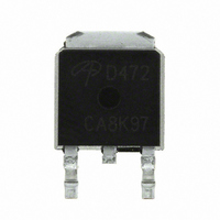
... AOD472 N-Channel Enhancement Mode Field Effect Transistor General Description The AOD472 uses advanced trench technology and design to provide excellent R with low gate DS(ON) charge. This device is suitable for use in PWM, load switching and general purpose applications. TO-252 D-PAK Top View Absolute Maximum Ratings T =25° ...
Page 2
... AOD472 Electrical Characteristics (T =25°C unless otherwise noted) J Symbol Parameter STATIC PARAMETERS BV Drain-Source Breakdown Voltage DSS I Zero Gate Voltage Drain Current DSS I Gate-Body leakage current GSS V Gate Threshold Voltage GS(th state drain current D(ON) R Static Drain-Source On-Resistance DS(ON) g Forward Transconductance FS V Diode Forward Voltage ...
Page 3
... AOD472 TYPICAL ELECTRICAL AND THERMAL CHARACTERISTICS 200 10V 160 6V 120 80 3. (Volts) DS Fig 1: On-Region Characteristics (A) D Figure 3: On-Resistance vs. Drain Current and Gate Voltage 25° (Volts) GS Figure 5: On-Resistance vs. Gate-Source Voltage Alpha & Omega Semiconductor, Ltd 4. 1.8 1.6 =4.5V 1.4 GS 1.2 ...
Page 4
... AOD472 TYPICAL ELECTRICAL AND THERMAL CHARACTERISTICS =12. =20A (nC) g Figure 7: Gate-Charge Characteristics 1000 T =175°C, T =25°C J(Max) C 100 R DS(ON) limited 0.1 0 (Volts) DS Figure 9: Maximum Forward Biased Safe Operating Area (Note θJC θJC J, =2.5°C/W θJC 1 0.1 Single Pulse 0.01 0.00001 ...
Page 5
... AOD472 TYPICAL ELECTRICAL AND THERMAL CHARACTERISTICS 100 =150° 0.000001 0.00001 Time in avalanche, t Figure 12: Single Pulse Avalanche capability (°C) CASE Figure 14: Current De-rating (Note θJA θJA R =50°C/W 1 θJA 0.1 0.01 Single Pulse 0.001 0.00001 0.0001 Figure 16: Normalized Maximum Transient Thermal Impedance (Note H) Alpha & ...
Page 6
... AOD472 ircu it & Vds DUT Vgs Rg Vgs U nc lam ctive S w itch ing ( ircu it & Isd Alpha & Omega Semiconductor, Ltd Resistive Switching Test Circuit & Waveforms Vds + Vdd VDC - Vgs d(on 1 ircu it & 90% 10 d(off) t off dI/ www.aosmd.com ...