SI7465DP-T1-E3 Vishay, SI7465DP-T1-E3 Datasheet - Page 7
SI7465DP-T1-E3
Manufacturer Part Number
SI7465DP-T1-E3
Description
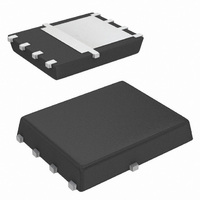
MOSFET P-CH 60V 3.2A PPAK 8SOIC
Manufacturer
Vishay
Series
TrenchFET®r
Type
Power MOSFETr
Specifications of SI7465DP-T1-E3
Transistor Polarity
P-Channel
Fet Type
MOSFET P-Channel, Metal Oxide
Fet Feature
Logic Level Gate
Rds On (max) @ Id, Vgs
64 mOhm @ 5A, 10V
Drain To Source Voltage (vdss)
60V
Current - Continuous Drain (id) @ 25° C
3.2A
Vgs(th) (max) @ Id
3V @ 250µA
Gate Charge (qg) @ Vgs
40nC @ 10V
Power - Max
1.5W
Mounting Type
Surface Mount
Package / Case
PowerPAK® SO-8
Minimum Operating Temperature
- 55 C
Configuration
Single Quad Drain Triple Source
Resistance Drain-source Rds (on)
0.064 Ohm @ 10 V
Drain-source Breakdown Voltage
60 V
Gate-source Breakdown Voltage
+/- 20 V
Continuous Drain Current
3.2 A
Power Dissipation
1500 mW
Maximum Operating Temperature
+ 150 C
Mounting Style
SMD/SMT
Continuous Drain Current Id
-5A
Drain Source Voltage Vds
-60V
On Resistance Rds(on)
80mohm
Rds(on) Test Voltage Vgs
20V
Threshold Voltage Vgs Typ
-3V
Number Of Elements
1
Polarity
P
Channel Mode
Enhancement
Drain-source On-res
0.064Ohm
Drain-source On-volt
60V
Gate-source Voltage (max)
±20V
Operating Temp Range
-55C to 150C
Operating Temperature Classification
Military
Mounting
Surface Mount
Pin Count
8
Package Type
PowerPAK SO
Lead Free Status / RoHS Status
Lead free / RoHS Compliant
Lead Free Status / RoHS Status
Lead free / RoHS Compliant, Lead free / RoHS Compliant
Other names
SI7465DP-T1-E3TR
Available stocks
Company
Part Number
Manufacturer
Quantity
Price
Company:

Part Number:
SI7465DP-T1-E3
Manufacturer:
Vishay/Siliconix
Quantity:
128 507
Company:
Part Number:
SI7465DP-T1-E3
Manufacturer:
VISHAY
Quantity:
21 676
Part Number:
SI7465DP-T1-E3
Manufacturer:
VISHAY/威世
Quantity:
20 000


Wharton McDaniel
MOSFETs for switching applications are now available
with die on resistances around 1 mΩ and with the
capability to handle 85 A. While these die capabilities
represent a major advance over what was available
just a few years ago, it is important for power MOSFET
packaging technology to keep pace. It should be obvi-
ous that degradation of a high performance die by the
package is undesirable. PowerPAK is a new package
technology that addresses these issues. In this appli-
cation note, PowerPAK’s construction is described.
Following this mounting information is presented
including land patterns and soldering profiles for max-
imum reliability. Finally, thermal and electrical perfor-
mance is discussed.
THE PowerPAK PACKAGE
The PowerPAK package was developed around the
SO-8 package (Figure 1). The PowerPAK SO-8 uti-
lizes the same footprint and the same pin-outs as the
standard SO-8. This allows PowerPAK to be substi-
tuted directly for a standard SO-8 package. Being a
leadless package, PowerPAK SO-8 utilizes the entire
SO-8 footprint, freeing space normally occupied by the
leads, and thus allowing it to hold a larger die than a
standard SO-8. In fact, this larger die is slightly larger
than a full sized DPAK die. The bottom of the die attach
pad is exposed for the purpose of providing a direct,
low resistance thermal path to the substrate the device
is mounted on. Finally, the package height is lower
than the standard SO-8, making it an excellent choice
for applications with space constraints.
Document Number 71622
28-Feb-06
PowerPAK
Figure 1. PowerPAK 1212 Devices
®
SO-8 Mounting and Thermal Considerations
PowerPAK SO-8 SINGLE MOUNTING
The PowerPAK single is simple to use. The pin
arrangement (drain, source, gate pins) and the pin
dimensions are the same as standard SO-8 devices
(see Figure 2). Therefore, the PowerPAK connection
pads match directly to those of the SO-8. The only dif-
ference is the extended drain connection area. To take
immediate advantage of the PowerPAK SO-8 single
devices, they can be mounted to existing SO-8 land
patterns.
The minimum land pattern recommended to take full
advantage of the PowerPAK thermal performance see
Application Note 826, Recommended Minimum Pad
Patterns With Outline Drawing Access for Vishay Sili-
conix MOSFETs. Click on the PowerPAK SO-8 single
in the index of this document.
In this figure, the drain land pattern is given to make full
contact to the drain pad on the PowerPAK package.
This land pattern can be extended to the left, right, and
top of the drawn pattern. This extension will serve to
increase the heat dissipation by decreasing the ther-
mal resistance from the foot of the PowerPAK to the
PC board and therefore to the ambient. Note that
increasing the drain land area beyond a certain point
will yield little decrease in foot-to-board and foot-to-
ambient thermal resistance. Under specific conditions
of board configuration, copper weight and layer stack,
experiments have found that more than about 0.25 to
0.5 in
land) will yield little improvement in thermal perfor-
mance.
2
of additional copper (in addition to the drain
Standard SO-8
Figure 2.
PowerPAK SO-8
Vishay Siliconix
www.vishay.com
AN821
1
Related parts for SI7465DP-T1-E3
Image
Part Number
Description
Manufacturer
Datasheet
Request
R

Part Number:
Description:
P-channel 60-v D-s Mosfet
Manufacturer:
Vishay
Datasheet:

Part Number:
Description:
MOSFET P-CH 60V 3.2A PPAK 8SOIC
Manufacturer:
Vishay
Datasheet:
Part Number:
Description:
357-036-542-201 CARDEDGE 36POS DL .156 BLK LOPRO
Manufacturer:
Vishay
Datasheet:
Part Number:
Description:
357-036-542-201 CARDEDGE 36POS DL .156 BLK LOPRO
Manufacturer:
Vishay
Datasheet:
Part Number:
Description:
357-036-542-201 CARDEDGE 36POS DL .156 BLK LOPRO
Manufacturer:
Vishay
Datasheet:
Part Number:
Description:
357-036-542-201 CARDEDGE 36POS DL .156 BLK LOPRO
Manufacturer:
Vishay
Datasheet:
Part Number:
Description:
357-036-542-201 CARDEDGE 36POS DL .156 BLK LOPRO
Manufacturer:
Vishay
Datasheet:
Part Number:
Description:
357-036-542-201 CARDEDGE 36POS DL .156 BLK LOPRO
Manufacturer:
Vishay
Datasheet:
Part Number:
Description:
357-036-542-201 CARDEDGE 36POS DL .156 BLK LOPRO
Manufacturer:
Vishay
Datasheet:
Part Number:
Description:
357-036-542-201 CARDEDGE 36POS DL .156 BLK LOPRO
Manufacturer:
Vishay
Datasheet:
Part Number:
Description:
357-036-542-201 CARDEDGE 36POS DL .156 BLK LOPRO
Manufacturer:
Vishay
Datasheet:
Part Number:
Description:
357-036-542-201 CARDEDGE 36POS DL .156 BLK LOPRO
Manufacturer:
Vishay
Datasheet:
Part Number:
Description:
357-036-542-201 CARDEDGE 36POS DL .156 BLK LOPRO
Manufacturer:
Vishay
Datasheet:
Part Number:
Description:
357-036-542-201 CARDEDGE 36POS DL .156 BLK LOPRO
Manufacturer:
Vishay
Datasheet:
Part Number:
Description:
357-036-542-201 CARDEDGE 36POS DL .156 BLK LOPRO
Manufacturer:
Vishay
Datasheet: