STK22N6F3 STMicroelectronics, STK22N6F3 Datasheet
STK22N6F3
Specifications of STK22N6F3
Available stocks


Related parts for STK22N6F3


STK22N6F3 Summary of contents
Page 1
... April 2009 N-channel 60 V, 0.0055 Ω PolarPAK STripFET™ Power MOSFET R max DS(on) < 0.006 Ω DS(on) Figure 1. Bottom View Marking Package 2263 PolarPAK Doc ID 14850 Rev 2 STK22N6F3 ® PolarPAK Internal schematic diagram Top View Packaging ® Tape and reel www.st.com ® 1/15 15 ...
Page 2
... Contents Contents 1 Electrical ratings . . . . . . . . . . . . . . . . . . . . . . . . . . . . . . . . . . . . . . . . . . . . 3 2 Electrical characteristics . . . . . . . . . . . . . . . . . . . . . . . . . . . . . . . . . . . . . 4 2.1 Electrical characteristics (curves) 3 Test circuits 4 Package mechanical data . . . . . . . . . . . . . . . . . . . . . . . . . . . . . . . . . . . . 10 5 Revision history . . . . . . . . . . . . . . . . . . . . . . . . . . . . . . . . . . . . . . . . . . . 14 2/ Doc ID 14850 Rev 2 STK22N6F3 ...
Page 3
... STK22N6F3 1 Electrical ratings Table 2. Absolute maximum ratings Symbol V Drain-source voltage ( Gate-source voltage GS (1) I Drain current (continuous Drain current (continuous (2) I Drain current (pulsed) DM (1) P Total dissipation at T TOT Derating factor (3) E Single pulse avalanche energy AS T Operating junction temperature j T Storage temperature stg 1 ...
Page 4
... Parameter Test conditions =4.7 Ω Figure =4.7 Ω Figure 13 Doc ID 14850 Rev 2 Min. Typ 250 µ 0.0055 0.006 D Min. Typ. 2500 =0 - 536 0.9 Min. Typ STK22N6F3 Max. Unit - V 10 µA 100 µA 200 nA ± Ω Max. Unit Ω - Max. Unit ...
Page 5
... STK22N6F3 Table 7. Source drain diode Symbol Source-drain current I SD Source-drain current (1) I SDM (pulsed) (2) V Forward on voltage SD t Reverse recovery time rr Q Reverse recovery charge rr I Reverse recovery current RRM 1. Pulse width limited by package 2. Pulsed: pulse duration = 300µs, duty cycle 1.5% ...
Page 6
... V ( temperaure Figure 7. AM03400v1 R DS(on) 75 100 125 150 T (°C) J Doc ID 14850 Rev 2 Thermal impedance Transfer characteristics I D ( Static drain-source on resistance (Ω) I =11A D 5.8 V =10V GS 5.7 5.6 5.5 5.4 5.3 5.2 5.1 5 STK22N6F3 AM03399v1 8 V (V) GS AM03891v1 20 I (A) D ...
Page 7
... STK22N6F3 Figure 8. Gate charge vs gate-source voltage Figure ( =48V DD I =22A Figure 10. Normalized gate threshold voltage vs temperature V GS(th) (norm) 1.1 1.0 0.9 0.8 0.7 0.6 0.5 0.4 - Figure 12. Source-drain diode forward characteristics V SD (V) 0.90 0.80 0.70 0.60 0. AM03892v1 6010 5010 4010 3010 ...
Page 8
... AM01468v1 Figure 16. Unclamped inductive load test 3.3 1000 µF µ AM01470v1 Figure 18. Switching time waveform V (BR)DSS 10% 0 AM01472v1 Doc ID 14850 Rev 2 STK22N6F3 12V 47kΩ 100nF I =CONST G 100Ω GMAX 2200 µF 2.7kΩ 47kΩ 1kΩ circuit 2200 3.3 µ ...
Page 9
... STK22N6F3 Figure 19. Gate charge waveform Vds Vgs(th) Qgs1 Qgs2 Qgd Id Vgs Doc ID 14850 Rev 2 Test circuits 9/15 ...
Page 10
... Package mechanical data 4 Package mechanical data In order to meet environmental requirements, ST offers these devices in different grades of ® ECOPACK packages, depending on their level of environmental compliance. ECOPACK specifications, grade definitions and product status are available at: www.st.com. ECOPACK trademark. 10/15 Doc ID 14850 Rev 2 STK22N6F3 ® ...
Page 11
... STK22N6F3 Table 8. PolarPAK Ref < ® (option “L”) mechanical data mm Min. Typ. Max. 0.75 0.80 0.85 0.05 0.48 0.58 0.68 0.41 0.51 0.61 2.19 2.29 2.39 0.89 1.04 1.19 0.23 0.33 0.43 0.20 0.25 0.30 6 6.15 6.30 5.74 5.89 6.04 5.01 5 ...
Page 12
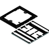
... Package mechanical data Figure 20. PolarPAK 12/15 ® (option “L”) drawings Doc ID 14850 Rev 2 STK22N6F3 ...
Page 13
... STK22N6F3 Figure 21. Recommended PAD layout Doc ID 14850 Rev 2 Package mechanical data 13/15 ...
Page 14
... Revision history 5 Revision history Table 9. Document revision history Date 01-Jul-2008 16-Apr-2009 14/15 Revision 1 First release 2 Document status promoted from preliminary data to datasheet Doc ID 14850 Rev 2 STK22N6F3 Changes ...
Page 15
... STK22N6F3 Information in this document is provided solely in connection with ST products. STMicroelectronics NV and its subsidiaries (“ST”) reserve the right to make changes, corrections, modifications or improvements, to this document, and the products and services described herein at any time, without notice. All ST products are sold pursuant to ST’s terms and conditions of sale. ...