IRFBF20LPBF Vishay, IRFBF20LPBF Datasheet - Page 3
IRFBF20LPBF
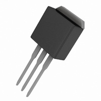
Manufacturer Part Number
IRFBF20LPBF
Description
MOSFET N-CH 900V 1.7A TO-262
Manufacturer
Vishay
Specifications of IRFBF20LPBF
Transistor Polarity
N-Channel
Fet Type
MOSFET N-Channel, Metal Oxide
Fet Feature
Standard
Rds On (max) @ Id, Vgs
8 Ohm @ 1A, 10V
Drain To Source Voltage (vdss)
900V
Current - Continuous Drain (id) @ 25° C
1.7A
Vgs(th) (max) @ Id
4V @ 250µA
Gate Charge (qg) @ Vgs
38nC @ 10V
Input Capacitance (ciss) @ Vds
490pF @ 25V
Power - Max
3.1W
Mounting Type
Through Hole
Package / Case
I²Pak, TO-262 (3 straight leads + tab)
Minimum Operating Temperature
- 55 C
Configuration
Single
Resistance Drain-source Rds (on)
8 Ohm @ 10 V
Drain-source Breakdown Voltage
900 V
Gate-source Breakdown Voltage
+/- 20 V
Continuous Drain Current
1.7 A
Power Dissipation
3100 mW
Maximum Operating Temperature
+ 150 C
Mounting Style
Through Hole
Continuous Drain Current Id
1.7A
Drain Source Voltage Vds
900V
On Resistance Rds(on)
8ohm
Rds(on) Test Voltage Vgs
10V
Leaded Process Compatible
Yes
Peak Reflow Compatible (260 C)
Yes
Rohs Compliant
Yes
Lead Free Status / RoHS Status
Lead free / RoHS Compliant
Lead Free Status / RoHS Status
Lead free / RoHS Compliant, Lead free / RoHS Compliant
Other names
*IRFBF20LPBF


Notes
a. Repetitive rating; pulse width limited by maximum junction temperature (see fig. 11).
b. Pulse width 300 μs; duty cycle 2 %.
c. Uses IRFBF20/SiHFBF20 data and test conditions.
TYPICAL CHARACTERISTICS (25 °C, unless otherwise noted)
Document Number: 91121
S10-2433-Rev. A, 25-Oct-10
SPECIFICATIONS (T
PARAMETER
Drain-Source Body Diode Characteristics
Continuous Source-Drain Diode Current
Pulsed Diode Forward Current
Body Diode Voltage
Body Diode Reverse Recovery Time
Body Diode Reverse Recovery Charge
Forward Turn-On Time
Fig. 1 - Typical Output Characteristics
J
= 25 °C, unless otherwise noted)
a
IRFBF20S, SiHFBF20S, IRFBF20L, SiHFBF20L
SYMBOL
V
I
Q
t
SM
I
t
SD
on
S
rr
rr
MOSFET symbol
showing the
integral reverse
p - n junction diode
T
J
= 25 °C, I
T
Intrinsic turn-on time is negligible (turn-on is dominated by L
J
= 25 °C, I
TEST CONDITIONS
F
= 1.7 A, dI/dt = 100 A/μs
S
= 1.7 A, V
Fig. 2 - Typical Output Characteristics
GS
G
= 0 V
b
D
S
b
MIN.
-
-
-
-
-
Vishay Siliconix
TYP.
0.85
350
-
-
-
www.vishay.com
MAX.
530
1.7
6.8
1.5
1.3
S
and L
D
UNIT
)
μC
ns
A
V
3
Related parts for IRFBF20LPBF
Image
Part Number
Description
Manufacturer
Datasheet
Request
R

Part Number:
Description:
MOSFET N-CH 900V 1.7A TO-220AB
Manufacturer:
Vishay
Datasheet:

Part Number:
Description:
357-036-542-201 CARDEDGE 36POS DL .156 BLK LOPRO
Manufacturer:
Vishay
Datasheet:
Part Number:
Description:
357-036-542-201 CARDEDGE 36POS DL .156 BLK LOPRO
Manufacturer:
Vishay
Datasheet:
Part Number:
Description:
357-036-542-201 CARDEDGE 36POS DL .156 BLK LOPRO
Manufacturer:
Vishay
Datasheet:
Part Number:
Description:
357-036-542-201 CARDEDGE 36POS DL .156 BLK LOPRO
Manufacturer:
Vishay
Datasheet:
Part Number:
Description:
357-036-542-201 CARDEDGE 36POS DL .156 BLK LOPRO
Manufacturer:
Vishay
Datasheet:
Part Number:
Description:
357-036-542-201 CARDEDGE 36POS DL .156 BLK LOPRO
Manufacturer:
Vishay
Datasheet:
Part Number:
Description:
357-036-542-201 CARDEDGE 36POS DL .156 BLK LOPRO
Manufacturer:
Vishay
Datasheet:
Part Number:
Description:
357-036-542-201 CARDEDGE 36POS DL .156 BLK LOPRO
Manufacturer:
Vishay
Datasheet:
Part Number:
Description:
357-036-542-201 CARDEDGE 36POS DL .156 BLK LOPRO
Manufacturer:
Vishay
Datasheet:
Part Number:
Description:
357-036-542-201 CARDEDGE 36POS DL .156 BLK LOPRO
Manufacturer:
Vishay
Datasheet:
Part Number:
Description:
357-036-542-201 CARDEDGE 36POS DL .156 BLK LOPRO
Manufacturer:
Vishay
Datasheet:
Part Number:
Description:
357-036-542-201 CARDEDGE 36POS DL .156 BLK LOPRO
Manufacturer:
Vishay
Datasheet:
Part Number:
Description:
357-036-542-201 CARDEDGE 36POS DL .156 BLK LOPRO
Manufacturer:
Vishay
Datasheet:
Part Number:
Description:
357-036-542-201 CARDEDGE 36POS DL .156 BLK LOPRO
Manufacturer:
Vishay
Datasheet: