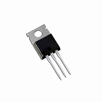
IRFB4310ZPBF International Rectifier, IRFB4310ZPBF Datasheet - Page 7

IRFB4310ZPBF
Manufacturer Part Number
IRFB4310ZPBF
Description
MOSFET N-CH 100V 120A TO-220AB
Manufacturer
International Rectifier
Series
HEXFET®r
Specifications of IRFB4310ZPBF
Fet Type
MOSFET N-Channel, Metal Oxide
Fet Feature
Standard
Rds On (max) @ Id, Vgs
6 mOhm @ 75A, 10V
Drain To Source Voltage (vdss)
100V
Current - Continuous Drain (id) @ 25° C
120A
Vgs(th) (max) @ Id
4V @ 150µA
Gate Charge (qg) @ Vgs
170nC @ 10V
Input Capacitance (ciss) @ Vds
6860pF @ 50V
Power - Max
250W
Mounting Type
Through Hole
Package / Case
TO-220-3 (Straight Leads)
Current, Drain
120 A
Gate Charge, Total
120 nC
Package Type
TO-220AB
Polarization
N-Channel
Power Dissipation
250 W
Resistance, Drain To Source On
4.8 Milliohms
Temperature, Operating, Maximum
+175 °C
Temperature, Operating, Minimum
-55 °C
Time, Turn-off Delay
55 ns
Time, Turn-on Delay
20 ns
Transconductance, Forward
150 S
Voltage, Breakdown, Drain To Source
100 V
Voltage, Forward, Diode
1.3 V
Voltage, Gate To Source
±20 V
Transistor Polarity
N-Channel
Drain-source Breakdown Voltage
100 V
Gate-source Breakdown Voltage
20 V
Continuous Drain Current
127 A
Mounting Style
Through Hole
Gate Charge Qg
120 nC
Lead Free Status / RoHS Status
Lead free / RoHS Compliant
Available stocks
Company
Part Number
Manufacturer
Quantity
Price
Part Number:
IRFB4310ZPBF
Manufacturer:
IR
Quantity:
20 000
www.irf.com
0
Fig 22a. Unclamped Inductive Test Circuit
Fig 23a. Switching Time Test Circuit
Fig 24a. Gate Charge Test Circuit
‚
+
-
R G
20K
20V
V
1K
V DS
GS
D.U.T
t p
≤ 0.1 %
≤ 1
Fig 21.
I AS
D.U.T
0.01 Ω
L
S
ƒ
+
-
•
•
•
•
DUT
SD
•
•
•
L
15V
DRIVER
-
„
G
+
-
+
-
V DD
+
VCC
A
+
-
Re-Applied
Voltage
Reverse
Recovery
Current
90%
Fig 22b. Unclamped Inductive Waveforms
V
10%
V
Driver Gate Drive
D.U.T. I
D.U.T. V
Inductor Curent
DS
Fig 23b. Switching Time Waveforms
GS
I
Fig 24b. Gate Charge Waveform
AS
Id
for HEXFET
P.W.
SD
DS
Vgs
Waveform
Waveform
t
d(on)
Ripple ≤ 5%
Body Diode
Period
Body Diode Forward
t
r
Diode Recovery
Qgodr
®
Current
t p
Power MOSFETs
dv/dt
Forward Drop
di/dt
t
d(off)
Qgd
D =
Period
V
P.W.
t
(BR)DSS
f
Qgs2
Vgs(th)
Vds
Qgs1
V
V
I
SD
GS
DD
=10V
7


