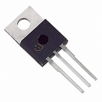
SPP04N50C3 Infineon Technologies, SPP04N50C3 Datasheet
首页 Discrete Semiconductor Products MOSFETs, GaNFETs - Single SPP04N50C3
Manufacturer Part Number
SPP04N50C3
Description
MOSFET N-CH 560V 4.5A TO-220AB
Manufacturer
Infineon Technologies
Specifications of SPP04N50C3
Package / Case
TO-220AB
Fet Type
MOSFET N-Channel, Metal Oxide
Fet Feature
Standard
Rds On (max) @ Id, Vgs
950 mOhm @ 2.8A, 10V
Drain To Source Voltage (vdss)
560V
Current - Continuous Drain (id) @ 25° C
4.5A
Vgs(th) (max) @ Id
3.9V @ 200µA
Gate Charge (qg) @ Vgs
22nC @ 10V
Input Capacitance (ciss) @ Vds
470pF @ 25V
Power - Max
50W
Mounting Type
Through Hole
Minimum Operating Temperature
- 55 C
Configuration
Single
Transistor Polarity
N-Channel
Resistance Drain-source Rds (on)
0.95 Ohm @ 10 V
Drain-source Breakdown Voltage
500 V
Gate-source Breakdown Voltage
+/- 20 V
Continuous Drain Current
4.5 A
Power Dissipation
50000 mW
Maximum Operating Temperature
+ 150 C
Mounting Style
Through Hole
Continuous Drain Current Id
4.5A
Drain Source Voltage Vds
500V
On Resistance Rds(on)
1.5ohm
Rds(on) Test Voltage Vgs
10V
Threshold Voltage Vgs Typ
3V
Rohs Compliant
Yes
Lead Free Status / RoHS Status
Lead free / RoHS Compliant
Lead Free Status / RoHS Status
Lead free / RoHS Compliant, Lead free / RoHS Compliant
Other names
SP000014478
Available stocks
Manufacturer:
INFINEON/英飞凌
Rev. 2.5
T
T
Gate source voltage
Power dissipation,
Reverse diode dv/dt
•
•
•
•
•
•
• G
C
C
V
V
DD
DD
T
C
G
7)
G
t
= 25°C
p
T
jmax
SP000216298
T
T
P
jmax
jmax
dv/dt
E
V
V
P
AR
GS
GS
tot
P-TO220-3-31
V
G
DS
±
T
jmax
1
2
1
3
±
G
2005-11-08
V/ns
Ω
Related parts for SPP04N50C3
SPP04N50C3 Summary of contents
Gate source voltage Power dissipation 25° Reverse diode dv/dt Rev. 2.5 SP000216298 T jmax E T ...
wavesoldering Rev. 2.5 R thJC R thJA V (BR)DSS µ ...
Transconductance Input capacitance Output capacitance Reverse transfer capacitance Turn-on delay time Rise time Turn-off delay time Fall time Gate to source charge Gate to drain charge 7 I <=I , di/dt<=400A/us DClink Identical low-side and high-side switch. ...
Inverse diode direct current, pulsed Reverse recovery time Reverse recovery charge Peak reverse recovery current Rev rrm 2005-11-08 ...
Rev. 2 tot 2005-11-08 ...
Rev. 2 2005-11-08 3 ...
Ω ≥ Rev. 2.5 Ω 2005-11-08 ...
Rev. 2.5 ≤ (BR)DSS 2005-11-08 3 ...
oss Rev. 2 2005-11-08 ...
Rev. 2 2005-11-08 ...
... PG-TO220-3-1, PG-TO220-3-21 Rev. 2.5 Page 11 SPP04N50C3 SPA04N50C3 2005-11-08 ...
... PG-TO220-3-31 (FullPAK) Rev. 2.5 Page 12 SPP04N50C3 SPA04N50C3 2005-11-08 ...
Rev. 2 2005-11-08 ...
Related keywords
spp04 spp04n80c3 spp04n60s5 spp04n60c3 spp04n50c3 spp04n50 SPP04N50C3 datasheet SPP04N50C3 data sheet SPP04N50C3 pdf datasheet SPP04N50C3 component SPP04N50C3 part SPP04N50C3 distributor SPP04N50C3 RoHS SPP04N50C3 datasheet download


