BS270 Fairchild Semiconductor, BS270 Datasheet
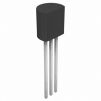
MOSFET N-CH 60V 400MA TO-92

BS270

Manufacturer Part Number
BS270
Description
MOSFET N-CH 60V 400MA TO-92
Manufacturer
Fairchild Semiconductor
Datasheet

Specifications of BS270

Fet Type
MOSFET N-Channel, Metal Oxide
Fet Feature
Logic Level Gate
Rds On (max) @ Id, Vgs
2 Ohm @ 500mA, 10V
Drain To Source Voltage (vdss)
60V
Current - Continuous Drain (id) @ 25° C
400mA
Vgs(th) (max) @ Id
2.5V @ 250µA
Input Capacitance (ciss) @ Vds
50pF @ 25V
Power - Max
625mW
Mounting Type
Through Hole
Package / Case
TO-92-3 (Standard Body), TO-226
Configuration
Single
Transistor Polarity
N-Channel
Resistance Drain-source Rds (on)
2 Ohm @ 10 V
Forward Transconductance Gfs (max / Min)
0.32 S
Drain-source Breakdown Voltage
60 V
Gate-source Breakdown Voltage
+/- 20 V
Continuous Drain Current
0.4 A
Power Dissipation
625 mW
Maximum Operating Temperature
+ 150 C
Mounting Style
Through Hole
Minimum Operating Temperature
- 55 C
Lead Free Status / RoHS Status
Lead free / RoHS Compliant
Gate Charge (qg) @ Vgs
-
Lead Free Status / Rohs Status
Lead free / RoHS Compliant

Available stocks

Company
Part Number
Manufacturer
Quantity
Price
Part Number:
BS270
Manufacturer:
FSC
Quantity:
656
Part Number:
BS270
Manufacturer:
FSC
Quantity:
15 000
Part Number:
BS270
Manufacturer:
FAIRCHILD/仙童
Quantity:
20 000
Company:
Part Number:
BS270
Quantity:
6 679
Company:
Part Number:
BS270
Quantity:
6 079
Company:
Part Number:
BS270-D74Z
Quantity:
347
Part Number:
BS270_D74Z
Manufacturer:
Fairchild Semiconductor
Quantity:
40 035
Absolute Maximum Ratings
Symbol
V
V
V
I
P
T
T
THERMAL CHARACTERISTICS
R
© 1997 Fairchild Semiconductor Corporation
D
These N-Channel enhancement mode field effect transistors
are produced using Fairchild's proprietary, high cell density,
DMOS technology. These products have been designed to
minimize on-state resistance while provide rugged, reliable,
and fast switching performance. They can be used in most
applications requiring up to 500mA DC. These products are
particularly suited for low voltage, low current applications such
as small servo motor control, power MOSFET gate drivers,
and other switching applications.
General Description
_____________
DSS
DGR
GSS
D
J
L
BS270
N-Channel Enhancement Mode Field Effect Transistor
,T
JA
STG
Parameter
Drain-Source Voltage
Drain-Gate Voltage (R
Gate-Source Voltage - Continuous
Drain Current - Continuous
Maximum Power Dissipation
Derate Above 25°C
Operating and Storage Temperature Range
Maximum Lead Temperature for Soldering
Purposes, 1/16" from Case for 10 Seconds
Thermal Resistacne, Junction-to-Ambient
___________________________________________________________________
- Pulsed
- Non Repetitive (tp < 50µs)
GS
< 1M )
T
A
= 25°C unless otherwise noted
Features
400mA, 60V. R
High density cell design for low R
Voltage controlled small signal switch.
Rugged and reliable.
High saturation current capability.
G
-55 to 150
BS270
2000
DS(ON)
400
625
300
200
60
60
5
20
40
= 2
D
S
@ V
GS
DS(ON)
= 10V.
.
April 1995
mW/°C
Units
°C/W
mW
mA
BS270.SAM
°C
°C
V
V
V

Related parts for BS270

BS270 Summary of contents

Page 1

... High density cell design for low R Voltage controlled small signal switch. Rugged and reliable. High saturation current capability 25°C unless otherwise noted A April 1995 = 10V. DS(ON DS(ON BS270 400 2000 625 5 -55 to 150 300 200 Units mW/°C °C °C °C/W BS270.SAM ...

Page 2

... 4 > DS(on 4 > DS(on) V > 200 mA DS DS(on 1.0 MHz 500 GEN 400 mA (Note Min Typ Max Units µ 500 µ - 2.1 2 3.5 1 0.14 0.225 2000 2700 mA 400 600 100 320 400 mA 2000 mA 0.88 1.2 V BS270.SAM ...

Page 3

... Figure 6. Gate Threshold Variation with . =4.0V 4.5 5 7.0 0.4 0.8 1.2 1 DRAIN CURRENT (A) D and Drain Current 10V 125°C J 25°C -55°C 0.4 0.8 1.2 1 DRAIN CURRENT (A) D Current and Temperature - JUNCTION TEMPERATURE (° Temperature 8.0 9 BS270.SAM ...

Page 4

... Figure 10. Gate Charge Characteristics t d(on OUT Output, V out DUT Input 10% Figure 12. Switching Waveforms 125°C J 25°C -55°C 0.4 0.6 0 BODY DIODE FORWARD VOLTAGE ( 25V 0.4 0.8 1.2 1 GATE CHARGE (nC off t t d(off) r 90% 90% 10% 10% 90% 50% 50% Pulse Width . 1 Inverted BS270.SAM ...

Page 5

... DRAIN-SOURCE VOLTAGE (V) DS Figure 13. Maximum Safe Operating Area 0.5 0.5 0.2 0.2 0.1 0.1 0.05 0.05 0.02 0.01 0.02 Single Pulse 0.01 0.0001 0.001 Figure 14. Transient Thermal Response Curve. (continued 0.01 0 TIME (sec ( (See Datasheet) JA P(pk ( Duty Cycle 100 300 BS270.SAM ...

Page 6

... PROELECTRON SERIES), 96 L34Z TO-92 STANDARD NO LEADCLIP STRAIGHT FOR: PKG 94 (PROELECTRON SERIES BCXXX, BFXXX, BSRXXX), 97, 98 FSCINT Label ©2001 Fairchild Semiconductor Corporation TAPE and REEL OPTION See Fig 2.0 for various Reeling Styles 5 Reels per Intermediate Box F63TNR Label Customized Label AMMO PACK OPTION See Fig 3 ...

Page 7

TO-92 Tape and Reel Data, continued TO-92 Reeling Style Configuration: Figure 2.0 Machine Option “A” (H) Style “A”, D26Z, D70Z (s/h) TO-92 Radial Ammo Packaging Configuration: Figure 3.0 FIRST WIRE OFF IS COLLECTOR ADHESIVE TAPE IS ON THE TOP SIDE ...

Page 8

TO-92 Tape and Reel Data, continued TO-92 Tape and Reel Taping Dimension Configuration: Figure 4 User Direction of Feed TO-92 Reel Configuration: Figure 5.0 ELECT ROSTATIC SEN SITIVE D EVICES F63TNR Label ...

Page 9

TO-92 Package Dimensions TO-92; TO-18 Reverse Lead Form (J35Z Option) (FS PKG Code 92, 94, 96) 1:1 Scale 1:1 on letter size paper Dimensions shown below are in: inches [millimeters] Part Weight per unit (gram): 0. Note: ...

Page 10

... TRADEMARKS The following are registered and unregistered trademarks Fairchild Semiconductor owns or is authorized to use and is not intended exhaustive list of all such trademarks. ACEx™ FASTr™ Bottomless™ GlobalOptoisolator™ CoolFET™ GTO™ CROSSVOLT™ HiSeC™ DOME™ ISOPLANAR™ ...

Related keywords