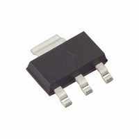
ZXMN7A11GTA Diodes Zetex, ZXMN7A11GTA Datasheet - Page 4

ZXMN7A11GTA
Manufacturer Part Number
ZXMN7A11GTA
Description
MOSFET N-CH 70V 3.8A SOT-223
Manufacturer
Diodes Zetex
Type
Power MOSFETr
Datasheet
1.ZXMN7A11GTA.pdf
(8 pages)
Specifications of ZXMN7A11GTA
Fet Type
MOSFET N-Channel, Metal Oxide
Fet Feature
Logic Level Gate
Rds On (max) @ Id, Vgs
130 mOhm @ 4.4A, 10V
Drain To Source Voltage (vdss)
70V
Current - Continuous Drain (id) @ 25° C
2.7A
Vgs(th) (max) @ Id
1V @ 250µA
Gate Charge (qg) @ Vgs
7.4nC @ 10V
Input Capacitance (ciss) @ Vds
298pF @ 40V
Power - Max
2W
Mounting Type
Surface Mount
Package / Case
SOT-223 (3 leads + Tab), SC-73, TO-261
Number Of Elements
1
Polarity
N
Channel Mode
Enhancement
Drain-source On-res
0.13Ohm
Drain-source On-volt
70V
Gate-source Voltage (max)
±20V
Continuous Drain Current
3.8A
Power Dissipation
3.9W
Operating Temp Range
-55C to 150C
Operating Temperature Classification
Military
Mounting
Surface Mount
Pin Count
3 +Tab
Package Type
SOT-223
Lead Free Status / RoHS Status
Lead free / RoHS Compliant
Other names
ZXMN7A11GTR
Available stocks
Company
Part Number
Manufacturer
Quantity
Price
Part Number:
ZXMN7A11GTA
Manufacturer:
ZETEX
Quantity:
20 000
Electrical characteristics (at T
Issue 1 - March 2006
© Zetex Semiconductors plc 2006
(*) Measured under pulsed conditions. Pulse width
(†) Switching characteristics are independent of operating junction temperature.
(‡) For design aid only, not subject to production testing.
NOTES:
Parameter
Static
Drain-source breakdown
voltage
Zero gate voltage drain current I
Gate-body leakage
Gate-source threshold voltage
Static drain-source on-state
resistance
Forward transconductance
Dynamic
Input capacitance
Output capacitance
Reverse transfer capacitance
Switching
Turn-on-delay time
Rise time
Turn-off delay time
Fall time
Total gate charge
Total gate charge
Gate-source charge
Gate drain charge
Source-drain diode
Diode forward voltage
Reverse recovery time
Reverse recovery charge
(‡)
(*)
(†)(‡)
(*)
(‡)
(‡)
(*)(‡)
Symbol
V
I
V
R
g
C
C
C
t
t
t
t
Q
Q
Q
Q
V
t
Q
DSS
GSS
d(on)
r
d(off)
f
rr
amb
fs
(BR)DSS
GS(th)
DS(on)
iss
oss
rss
SD
g
g
gs
gd
rr
= 25°C unless otherwise stated)
300 s; duty cycle
Min.
1.0
70
4
Typ.
4.66
11.5
4.35
1.06
0.85
19.8
298
1.9
5.8
7.4
1.8
35
21
14
2
Max.
0.13
0.19
0.95
100
2%.
1
Unit
nA
nC
nC
nC
nC
nC
pF
pF
pF
ns
ns
ns
ns
ns
V
V
S
V
A
ZXMN7A11G
Conditions
I
V
V
I
V
V
V
V
f=1MHz
V
R
V
I
V
I
T
V
T
di/dt=100A/ s
D
D
D
D
j
j
DS
GS
GS
GS
DS
DS
DD
G
DS
DS
GS
= 250 A, V
= 250 A, V
= 4.4A
= 4.4A
=25°C, I
=25°C, I
≅6.0 , V
= 70V, V
= 15V, I
= 40V, V
= 35V, V
=35V, V
=±20V, V
= 10V, I
= 4.5V, I
= 35V, I
=0V
www.zetex.com
S
S
= 2.5A,
= 2.5A,
D
GS
D
D
GS
D
GS
GS
GS
= 4.4A
= 4.4A
= 1A
DS
GS
DS
= 3.8A
= 10V
= 10V
=0V
=0V
= 5V
=0V
=V
=0V
GS


